Payment Method


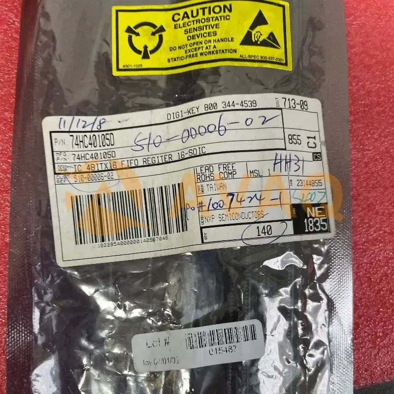
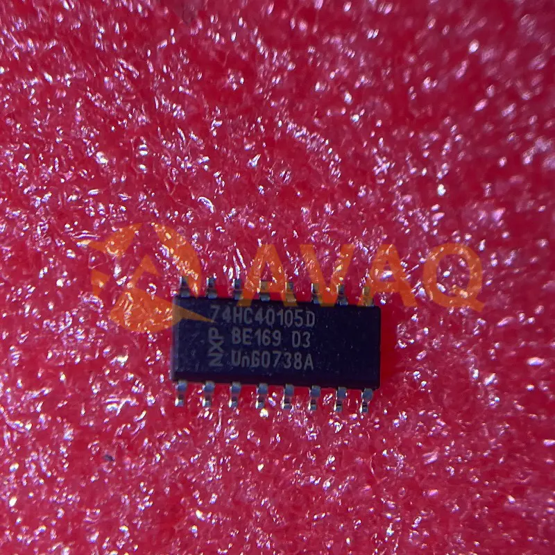
Registers 4BX16W FIFO REGISTER
SOP16Manufacturer:
Mfr.Part #:
74HC40105D
Datasheet:
Logic Type:
CMOS
Logic Family:
HC
Number Of Circuits:
Triple
Maximum Clock Frequency:
36 MHz
EDA/CAD Models:
All bill of materials (BOM) can be sent via email to ![]() [email protected],
or fill below form to Quote for 74HC40105D, guaranteed quotes back within
[email protected],
or fill below form to Quote for 74HC40105D, guaranteed quotes back within
![]() 12hr.
12hr.
Please fill in the short form below and we will provide you the quotation immediately.
INTEGRATED CIRCUITS DATA SHEET FAMILY SPECIFICATIONS HCMOS family characteristics March 1988 File under Integrated Circuits, IC06 Philips Semiconductors HCMOS family characteristics GENERAL These family specifications cover the common electrical ratings and characteristics of the entire HCMOS 74HC/HCT/HCU family, unless otherwise specified in the individual device data sheet. INTRODUCTION The 74HC/HCT/HCU high-speed Si-gate CMOS logic family combines the low power advantages of the HE4000B family with the high speed and drive capability of the low power Schottky TTL (LSTTL). The family will have the same pin-out as the 74 series and provide the same circuit functions. In these families are included several HE4000B family circuits which do not have TTL counterparts, and some special circuits. The basic family of buffered devices, designated as XX74HCXXXXX, will operate at CMOS input logic levels for high noise immunity, negligible typical quiescent supply and input current. It is operated from a power supply of 2 to 6 V. FAMILY SPECIFICATIONS A subset of the family, designated as XX74HCTXXXXX, with the same features and functions as the “HC-types”, will operate at standard TTL power supply voltage (5 V ± 10%) and logic input levels (0.8 to 2.0 V) for use as pin-to-pin compatible CMOS replacements to reduce power consumption without loss of speed. These types are also suitable for converted switching from TTL to CMOS. Another subset, the XX74HCUXXXXX, consists of single-stage unbuffered CMOS compatible devices for application in RC or crystal controlled oscillators and other types of feedback circuits which operate in the linear mode. HANDLING MOS DEVICES Inputs and outputs are protected against electrostatic effects in a wide variety of device-handling situations. However, to be totally safe, it is desirable to take handling precautions into account (see also “HANDLING PRECAUTIONS”). RECOMMENDED OPERATING CONDITIONS FOR 74HC/HCT 74HC SYMBOL PARAMETER min. typ. VCC VI VO Tamb Tamb tr, tf DC supply voltage DC input voltage range DC output voltage range 2.0 0 0 5.0 max. 6.0 VCC VCC +85 +125 1000 6.0 500 400 Note 1. For analog switches, e.g. “4016”, “4051 series”, “4351 series”, “4066” and “4067”, the specified maximum operating supply voltage is 10 V. 6.0 500 ns min. typ. max. 4.5 0 0 −40 −40 5.0 5.5 VCC VCC +85 +125 V V V °C °C see DC and AC CHAR. per device VCC = 2.0 V VCC = 4.5 V VCC = 6.0 V 74HCT UNIT CONDITIONS operating ambient temperature range −40 operating ambient temperature range −40 input rise and fall times except for Schmitt-trigger inputs March 1988 2 Philips Semiconductors HCMOS family characteristics RECOMMENDED OPERATING CONDITIONS FOR 74HCU FAMILY SPECIFICATIONS 74HCU SYMBOL VCC VI VO Tamb Tamb PARAMETER min. typ. max. DC supply voltage DC input voltage range DC output voltage range operating ambient temperature range operating ambient temperature range 2.0 0 0 −40 −40 5.0 6.0 […]
| Product Category | Registers | Logic Type | CMOS |
| Logic Family | HC | Number of Circuits | Triple |
| Maximum Clock Frequency | 36 MHz | High Level Output Current | - 7.8 mA |
| Low Level Output Current | 7.8 mA | Supply Voltage - Max | 6 V |
| Supply Voltage - Min | 2 V | Minimum Operating Temperature | - 40 C |
| Maximum Operating Temperature | + 125 C | Height | 1.45 mm |
| Input Type | Single-Ended | Length | 10 mm |
| Mounting Style | SMD/SMT | Number of Channels | 4 |
| Number of Input Lines | 4 | Number of Output Lines | 4 |
| Operating Supply Voltage | 5 V | Output Type | 3-State |
| Polarity | Non-Inverting | Product Type | Registers |
| Quiescent Current | 8 uA | Reset Type | Asynchronous |
| Factory Pack Quantity | 50 | Subcategory | Logic ICs |
| Width | 4 mm | Part # Aliases | 74HC40105D,652 |
| Unit Weight | 0.008818 oz |
After-Sales & Settlement Related
 Payment
Payment Method


For alternative payment channels, please reach out to us at:
[email protected] Shipping & Packing
Shipping Method


AVAQ determines and packages all devices based on electrostatic discharge (ESD) and moisture sensitivity level (MSL) protection requirements.
 Warranty

365-Day Product
Quality Guarantee
We promise to provide 365 days quality assurance service for all our products.
| Qty. | Unit Price | Ext. Price |
|---|---|---|
| 1+ | - | - |
The prices below are for reference only.


Received but not yet checked check i will add feedback