Payment Method


Advanced FPGA technology with a capacity of 250K system gates
132-WFQFNManufacturer:
Microsemi Corporation
Mfr.Part #:
A3P250-QNG132
Datasheet:
Series:
ProASIC3
Programmabe:
Not Verified
Total RAM Bits:
36864
Number Of I/O:
87
EDA/CAD Models:
All bill of materials (BOM) can be sent via email to ![]() [email protected],
or fill below form to Quote for A3P250-QNG132, guaranteed quotes back within
[email protected],
or fill below form to Quote for A3P250-QNG132, guaranteed quotes back within
![]() 12hr.
12hr.
Please fill in the short form below and we will provide you the quotation immediately.
The A3P250-QNG132, part of the Actel Fusion family of FPGAs, is a powerful solution with 250,000 system gates and non-volatile flash-based technology. Its 132-pin QFN package offers a compact form factor, ideal for diverse applications such as industrial automation, automotive, and consumer electronics. With its balance of logic capacity and I/O flexibility, this FPGA is well-suited for a wide range of embedded system designs
| Series | ProASIC3 | Programmabe | Not Verified |
| Total RAM Bits | 36864 | Number of I/O | 87 |
| Number of Gates | 250000 | Voltage - Supply | 1.425V ~ 1.575V |
| Mounting Type | Surface Mount | Operating Temperature | 0°C ~ 85°C (TJ) |
| Base Product Number | A3P250 |
After-Sales & Settlement Related
 Payment
Payment Method


For alternative payment channels, please reach out to us at:
[email protected] Shipping & Packing
Shipping Method


AVAQ determines and packages all devices based on electrostatic discharge (ESD) and moisture sensitivity level (MSL) protection requirements.
 Warranty

365-Day Product
Quality Guarantee
We promise to provide 365 days quality assurance service for all our products.
| Qty. | Unit Price | Ext. Price |
|---|---|---|
| 1+ | - | - |
The prices below are for reference only.

C100
Issi
Video ICs 4MP H.265 Video Processor - 64MB DDR2, BGA85, 5mm x 6mm

NE555
Texas Instruments
100kHz operation frequency with low power consumption for long-lasting performance

CD4017
Onsemi
Compact digital counter for precision measurement application

74LS04
Onsemi
High-quality die for professional use only, unsurfaced and untested

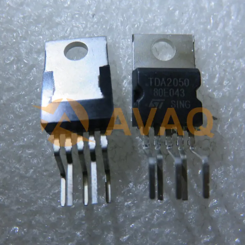
TDA2050
Stmicroelectronics
Effortlessly drives your speakers with crystal-clear sound and robust power