Payment Method


LEAD FREE A3P400-FGG144 Field Programmable Gate Array FPGA
144-LBGAManufacturer:
Microchip Technology
Mfr.Part #:
A3P400-FGG144
Datasheet:
Series:
ProASIC3
Programmabe:
Not Verified
Total RAM Bits:
55296
Number Of I/O:
97
EDA/CAD Models:
All bill of materials (BOM) can be sent via email to ![]() [email protected],
or fill below form to Quote for A3P400-FGG144, guaranteed quotes back within
[email protected],
or fill below form to Quote for A3P400-FGG144, guaranteed quotes back within
![]() 12hr.
12hr.
Please fill in the short form below and we will provide you the quotation immediately.
Representing the cutting edge of FPGA technology, the A3P400-FGG144 is a versatile solution for medium complexity logic functions. Its 144-pin FBGA package houses a powerhouse of 400,000 system gates, offering a wide range of applications in industrial, automotive, communication, and consumer electronics sectors. The FPGA's robust security features, including advanced encryption and authentication, ensure the safety of critical data and prevent unauthorized access
| Series | ProASIC3 | Programmabe | Not Verified |
| Total RAM Bits | 55296 | Number of I/O | 97 |
| Number of Gates | 400000 | Voltage - Supply | 1.425V ~ 1.575V |
| Mounting Type | Surface Mount | Operating Temperature | 0°C ~ 85°C (TJ) |
| Base Product Number | A3P400 |
After-Sales & Settlement Related
 Payment
Payment Method


For alternative payment channels, please reach out to us at:
[email protected] Shipping & Packing
Shipping Method


AVAQ determines and packages all devices based on electrostatic discharge (ESD) and moisture sensitivity level (MSL) protection requirements.
 Warranty

365-Day Product
Quality Guarantee
We promise to provide 365 days quality assurance service for all our products.
| Qty. | Unit Price | Ext. Price |
|---|---|---|
| 1+ | - | - |
The prices below are for reference only.

C100
Issi
Video ICs 4MP H.265 Video Processor - 64MB DDR2, BGA85, 5mm x 6mm

NE555
Texas Instruments
100kHz operation frequency with low power consumption for long-lasting performance

CD4017
Onsemi
Compact digital counter for precision measurement application

74LS04
Onsemi
High-quality die for professional use only, unsurfaced and untested

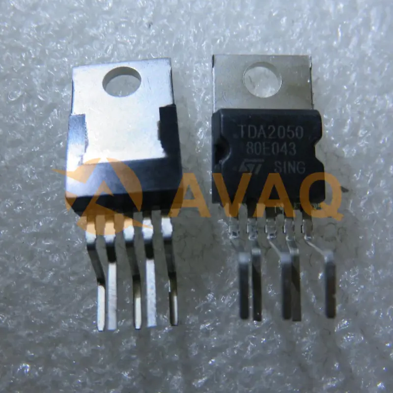
TDA2050
Stmicroelectronics
Effortlessly drives your speakers with crystal-clear sound and robust power