This website uses cookies. By using this site, you consent to the use of cookies. For more information, please take a look at our Privacy Policy.

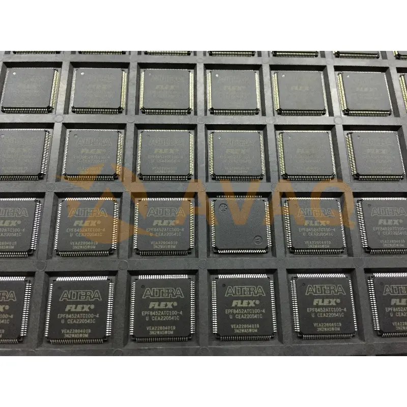
EPF8452ATC100-4 +BOM

Application: Electronic design and prototyping

EPF8452ATC100-4 General Description

The EPF8452ATC100-4 is a high-performance field-programmable gate array (FPGA) produced by Altera. Part of the MAX II family of FPGAs, it is tailored for demanding applications that require advanced performance and flexibility. With a package type of 100-pin thin quad flat pack (TQFP), this FPGA boasts a total of 4520 logic elements, making it suitable for complex tasks. Operating at a speed grade of 4, it can achieve a maximum internal frequency of 330 MHz, ensuring rapid processing and responsiveness

Key Features

  • Low-cost, high-density, register-rich CMOS programmable logic
  • device (PLD) family (see Table 1)
  • – 2,500 to 16,000 usable gates
  • – 282 to 1,500 registers
  • System-level features
  • – In-circuit reconfigurability (ICR) via external configuration
  • devices or intelligent controller
  • – Fully compliant with the peripheral component interconnect
  • Special Interest Group (PCI SIG) PCI Local Bus Specification,
  • Revision 2.2 for 5.0-V operation
  • – Built-in Joint Test Action Group (JTAG) boundary-scan test (BST)
  • circuitry compliant with IEEE Std. 1149.1-1990 on selected devices
  • – MultiVoltTM I/O interface enabling device core to run at 5.0 V,
  • while I/O pins are compatible with 5.0-V and 3.3-V logic levels
  • – Low power consumption (typical specification is 0.5 mA or less in
  • standby mode)
  • Flexible interconnect
  • – FastTrack® Interconnect continuous routing structure for fast,
  • predictable interconnect delays
  • – Dedicated carry chain that implements arithmetic functions such
  • as fast adders, counters, and comparators (automatically used by
  • software tools and megafunctions)
  • – Dedicated cascade chain that implements high-speed, high-fan-in
  • logic functions (automatically used by software tools and
  • megafunctions)
  • – Tri-state emulation that implements internal tri-state nets
  • Powerful I/O pins
  • Programmable output slew-rate control reduces switching noise
  • Peripheral register for fast setup and clock-to-output delay
  • Fabricated on an advanced SRAM process
  • Available in a variety of packages with 84 to 304 pins (see Table 2)
  • Software design support and automatic place-and-route provided by
  • the Altera® MAX+PLUS® II development system for Windows-based
  • PCs, as well as Sun SPARCstation, HP 9000 Series 700/800, and IBM
  • RISC System/6000 workstations
  • Additional design entry and simulation support provided by EDIF
  • 2 0 0 and 3 0 0 netlist files, library of parameterized modules (LPM),
  • Verilog HDL, VHDL, and other interfaces to popular EDA tools from
  • manufacturers such as Cadence, Exemplar Logic, Mentor Graphics,
  • OrCAD, Synopsys, Synplicity, and Veribest

Specifications

Programmabe Not Verified Number of LABs/CLBs 42
Number of Logic Elements/Cells 336 Total RAM Bits -
Number of I/O 68 Number of Gates 4000
Voltage - Supply 4.75V ~ 5.25V Mounting Type Surface Mount
Operating Temperature 0°C ~ 70°C (TA)

Service Policies and Others

After-Sales & Settlement Related

payment Payment

Payment Method

hsbc
TT/Wire Transfer
paypal
Paypal
wu
Western Union
mg
Money Gram

For alternative payment channels, please reach out to us at:

[email protected]
shipping Shipping & Packing

Shipping Method

fedex
Fedex
ups
UPS
dhl
DHL
tnt
NTN
Packing

AVAQ determines and packages all devices based on electrostatic discharge (ESD) and moisture sensitivity level (MSL) protection requirements.

Warranty Warranty

We promise to provide 365 days quality assurance service for all our products.

Reviews

You need to log in to reply. Sign In | Sign Up

In Stock: 4,349

Minimum Order: 1

Qty. Unit Price Ext. Price
1+ - -

The prices below are for reference only.