Payment Method


A dual flip-flop circuit used to synchronize and delay clock transition
14-SOIC(0.154",3.90mmWidth)Manufacturer:
National Semiconductor
Mfr.Part #:
JM4013BBDA
Datasheet:
Function:
Set(Preset) and Reset
Type:
D-Type
Output Type:
Complementary
Number Of Elements:
2
Send all BOMs to ![]() [email protected],
or fill out the form below for a quote on JM4013BBDA. Guaranteed response within
[email protected],
or fill out the form below for a quote on JM4013BBDA. Guaranteed response within
![]() 12hr.
12hr.
Please fill in the short form below and we will provide you the quotation immediately.
Flip Flop 2 Element D-Type 1 Bit Positive Edge 14-SOIC (0.154", 3.90mm Width)
| Series | - | Function | Set(Preset) and Reset |
| Type | D-Type | Output Type | Complementary |
| Number of Elements | 2 | Number of Bits per Element | 1 |
| Max Propagation Delay @ V, Max CL | 825ns @ 5V, 50pF | Trigger Type | Positive Edge |
| Current - Output High, Low | 15mA, 15mA | Voltage - Supply | 4.5V ~ 15V |
| Current - Quiescent (Iq) | 2.5 µA | Input Capacitance | 12 pF |
| Operating Temperature | -55°C ~ 125°C (TA) | Mounting Type | Surface Mount |
| Base Product Number | JM4013 |
After-Sales & Settlement Related
 Payment
Payment Method


For alternative payment channels, please reach out to us at:
[email protected] Shipping & Packing
Shipping Method


AVAQ determines and packages all devices based on electrostatic discharge (ESD) and moisture sensitivity level (MSL) protection requirements.
 Warranty

365-Day Product
Quality Guarantee
We promise to provide 365 days quality assurance service for all our products.
| Qty. | Unit Price | Ext. Price |
|---|---|---|
| 1+ | $10.313 | $10.31 |
| 200+ | $3.991 | $798.20 |
| 500+ | $3.852 | $1,926.00 |
| 1000+ | $3.782 | $3,782.00 |
The prices below are for reference only.
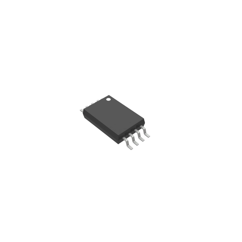
NE555
Texas Instruments
100kHz operation frequency with low power consumption for long-lasting performance
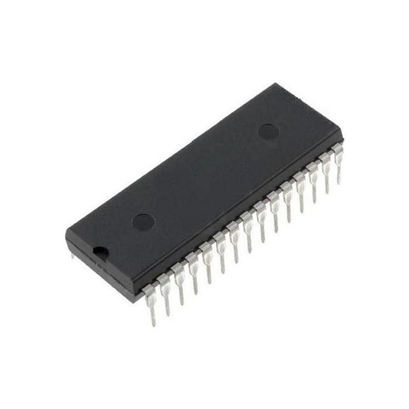
CD4017
Onsemi
Compact digital counter for precision measurement application

74LS04
Onsemi
High-quality die for professional use only, unsurfaced and untested
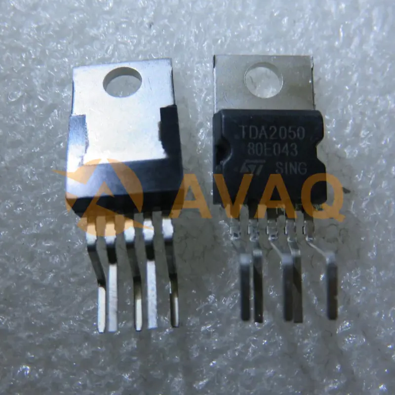
TDA2050
Stmicroelectronics
Effortlessly drives your speakers with crystal-clear sound and robust power
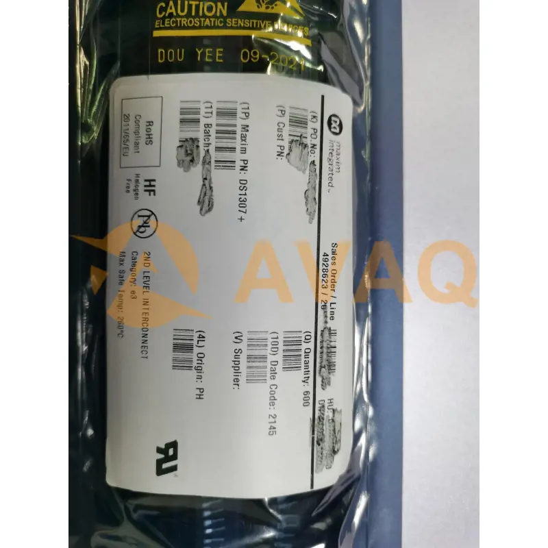
DS1307+
Analog Devices
I2C DIP-8 Real-time Clocks (RTC) ROHS