Payment Method


Ultra-low Bias Current, Precision CMOS Rail-to-Rail Input and Output Dual Operational Amplifier
SOIC (D)-8Manufacturer:
Mfr.Part #:
LMC6482IMX/NOPB
Datasheet:
Pbfree Code:
Yes
Part Life Cycle Code:
Active
Pin Count:
8
Reach Compliance Code:
compliant
EDA/CAD Models:
Send all BOMs to ![]() [email protected],
or fill out the form below for a quote on LMC6482IMX/NOPB. Guaranteed response within
[email protected],
or fill out the form below for a quote on LMC6482IMX/NOPB. Guaranteed response within
![]() 12hr.
12hr.
Please fill in the short form below and we will provide you the quotation immediately.
Elevate your designs with the exceptional features of the LMC6482IMX/NOPB, a dual operational amplifier designed by Texas Instruments. Boasting rail-to-rail input and output swings, this amplifier is a versatile choice for applications across different industries, including industrial, automotive, and consumer electronics. Its wide supply voltage range of 2.7V to 12V provides designers with the flexibility needed to create innovative solutions. With a low input offset voltage of 0.3mV and low input bias current of 0.01pA, the LMC6482IMX/NOPB ensures accurate and stable operation. Its high slew rate of 1.6V/μs and unity gain bandwidth of 2.8MHz make it well-suited for applications requiring fast response times. In addition, this amplifier offers low noise performance, with a typical input voltage noise of 16nV/√Hz, essential for maintaining signal integrity in critical applications. Packaged in a small outline package (SOIC) with integrated ESD protection, the LMC6482IMX/NOPB is not only easy to integrate into various circuit designs but also guarantees reliability and robust performance


| Source Content uid | LMC6482IMX/NOPB | Pbfree Code | Yes |
| Part Life Cycle Code | Active | Pin Count | 8 |
| Reach Compliance Code | compliant | ECCN Code | EAR99 |
| HTS Code | 8542.33.00.01 | Amplifier Type | OPERATIONAL AMPLIFIER |
| Architecture | VOLTAGE-FEEDBACK | Average Bias Current-Max (IIB) | 0.000004 µA |
| Bias Current-Max (IIB) @25C | 0.000004 µA | Common-mode Reject Ratio-Min | 70 dB |
| Common-mode Reject Ratio-Nom | 82 dB | Frequency Compensation | YES |
| Input Offset Current-Max (IIO) | 0.000002 µA | Input Offset Voltage-Max | 750 µV |
| JESD-30 Code | R-PDSO-G8 | JESD-609 Code | e3 |
| Length | 4.9 mm | Low-Bias | YES |
| Low-Offset | NO | Micropower | YES |
| Moisture Sensitivity Level | 1 | Neg Supply Voltage Limit-Max | |
| Neg Supply Voltage-Nom (Vsup) | Number of Functions | 2 | |
| Number of Terminals | 8 | Operating Temperature-Max | 85 °C |
| Operating Temperature-Min | -40 °C | Packing Method | TR |
| Peak Reflow Temperature (Cel) | 260 | Power | NO |
| Programmable Power | NO | Qualification Status | Not Qualified |
| Seated Height-Max | 1.75 mm | Slew Rate-Min | 0.63 V/us |
| Slew Rate-Nom | 1.3 V/us | Supply Current-Max | 1.4 mA |
| Supply Voltage Limit-Max | 16 V | Supply Voltage-Nom (Vsup) | 5 V |
| Surface Mount | YES | Technology | CMOS |
| Temperature Grade | INDUSTRIAL | Terminal Finish | Matte Tin (Sn) |
| Terminal Form | GULL WING | Terminal Pitch | 1.27 mm |
| Terminal Position | DUAL | Time@Peak Reflow Temperature-Max (s) | NOT SPECIFIED |
| Unity Gain BW-Nom | 1500 | Voltage Gain-Min | 10000 |
| Wideband | NO | Width | 3.9 mm |
After-Sales & Settlement Related
 Payment
Payment Method


For alternative payment channels, please reach out to us at:
[email protected] Shipping & Packing
Shipping Method


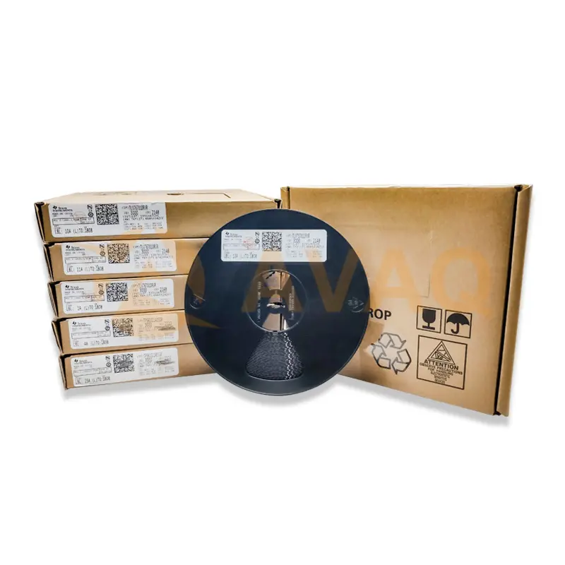
AVAQ determines and packages all devices based on electrostatic discharge (ESD) and moisture sensitivity level (MSL) protection requirements.
 Warranty

365-Day Product
Quality Guarantee
We promise to provide 365 days quality assurance service for all our products.
| Qty. | Unit Price | Ext. Price |
|---|---|---|
| 1+ | $1.181 | $1.18 |
| 10+ | $1.009 | $10.09 |
| 30+ | $0.915 | $27.45 |
| 100+ | $0.809 | $80.90 |
| 500+ | $0.647 | $323.50 |
| 1000+ | $0.627 | $627.00 |
The prices below are for reference only.