Payment Method


Low-noise jitter cleaner with 1840 to 2160-MHz VCO:2 outputs for 2VPEC/LVPEC+LVDS+LVCOMS
QFNManufacturer:
Mfr.Part #:
LMK04033BISQE/NOPB
Datasheet:
Function:
Cascaded PLLs
Number Of Outputs:
6
RMS Jitter (fs):
150
Output Frequency (min) (MHz):
0.45
EDA/CAD Models:
All bill of materials (BOM) can be sent via email to ![]() [email protected],
or fill below form to Quote for LMK04033BISQE/NOPB, guaranteed quotes back within
[email protected],
or fill below form to Quote for LMK04033BISQE/NOPB, guaranteed quotes back within
![]() 12hr.
12hr.
Please fill in the short form below and we will provide you the quotation immediately.
The LMK04000 family of precision clock conditioners provides low-noise jitter cleaning, clock multiplication and distribution without the need for high-performance voltage controlled crystal oscillators (VCXO) module. Using a cascaded PLLatinum architecture combined with an external crystal and varactor diode, the LMK04000 family provides sub-200 femtosecond (fs) root mean square (RMS) jitter performance.
The cascaded architecture consists of two high-performance phase-locked loops (PLL), a low-noise crystal oscillator circuit, and a high-performance voltage controlled oscillator (VCO). The first PLL (PLL1) provides a low-noise jitter cleaner function while the second PLL (PLL2) performs the clock generation. PLL1 can be configured to either work with an external VCXO module or use the integrated crystal oscillator with an external crystal and a varactor diode. When used with a very narrow loop bandwidth, PLL1 uses the superior close-in phase noise (offsets below 50 kHz) of the VCXO module or the crystal to clean the input clock. The output of PLL1 is used as the clean input reference to PLL2 where it locks the integrated VCO. The loop bandwidth of PLL2 can be optimized to clean the far-out phase noise (offsets above 50 kHz) where the integrated VCO outperforms the VCXO module or crystal used in PLL1.
The LMK04000 family features dual redundant inputs, five differential outputs, and an optional default-clock upon power up. The input block is equipped with loss of signal detection and automatic or manual selection of the reference clock. Each clock output consists of a programmable divider, a phase synchronization circuit, a programmable delay, and an LVDS, LVPECL, or LVCMOS output buffer. The default startup clock is available on CLKout2 and it can be used to provide an initial clock for the field-programmable gate array (FPGA) or microcontroller that programs the jitter cleaner during the system power up sequence.


| Function | Cascaded PLLs | Number of outputs | 6 |
| RMS jitter (fs) | 150 | Output frequency (min) (MHz) | 0.45 |
| Output frequency (max) (MHz) | 2160 | Input type | LVCMOS, LVDS, LVPECL |
| Output type | LVCMOS, LVDS, LVPECL | Supply voltage (min) (V) | 3.15 |
| Supply voltage (max) (V) | 3.45 | Features | Integrated VCO |
| Rating | Catalog | Operating temperature range (°C) | -40 to 85 |
| Number of input channels | 2 | feature-maximum-operating-supply-voltage-v | 3.45 |
| feature-minimum-operating-supply-voltage-v | 3.15 | feature-packaging | Tape and Reel |
| feature-rad-hard | feature-pin-count | 48 | |
| feature-cecc-qualified | No | feature-esd-protection | Yes |
| feature-escc-qualified | feature-military | No | |
| feature-aec-qualified | No | feature-aec-qualified-number | |
| feature-auto-motive | No | feature-p-pap | No |
| feature-eccn-code | EAR99 | feature-svhc | Yes |
| feature-svhc-exceeds-threshold | No |
After-Sales & Settlement Related
 Payment
Payment Method


For alternative payment channels, please reach out to us at:
[email protected] Shipping & Packing
Shipping Method


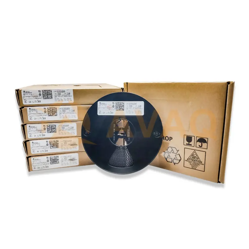
AVAQ determines and packages all devices based on electrostatic discharge (ESD) and moisture sensitivity level (MSL) protection requirements.
 Warranty

365-Day Product
Quality Guarantee
We promise to provide 365 days quality assurance service for all our products.
| Qty. | Unit Price | Ext. Price |
|---|---|---|
| 1+ | - | - |
The prices below are for reference only.