Payment Method


High-Speed LVDS Conversion Solutio
TSSOPManufacturer:
Mfr.Part #:
NB3N4666CDTR2G
Datasheet:
Case Outline:
948F-01
MSL Temp (°C):
260
Container Type:
REEL
EDA/CAD Models:
Send all BOMs to ![]() [email protected],
or fill out the form below for a quote on NB3N4666CDTR2G. Guaranteed response within
[email protected],
or fill out the form below for a quote on NB3N4666CDTR2G. Guaranteed response within
![]() 12hr.
12hr.
Please fill in the short form below and we will provide you the quotation immediately.
One standout feature of the NB3N4666C is its input fail-safe protection circuit, which ensures a reliable output voltage even under challenging conditions such as open-circuit, short, or terminated (100 Ω) inputs. This level of protection gives users peace of mind knowing that their data signals will be handled accurately and securely


| Status | Active | Case Outline | 948F-01 |
| MSL Temp (°C) | 260 | Container Type | REEL |
After-Sales & Settlement Related
 Payment
Payment Method


For alternative payment channels, please reach out to us at:
[email protected] Shipping & Packing
Shipping Method


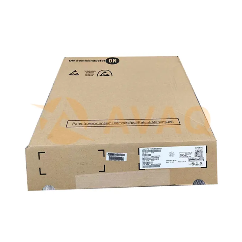
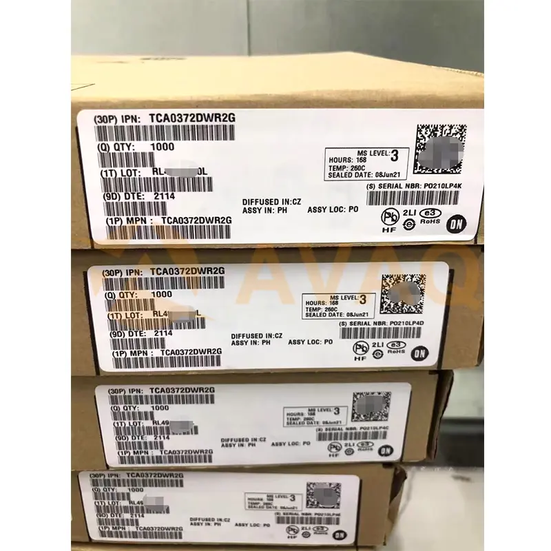
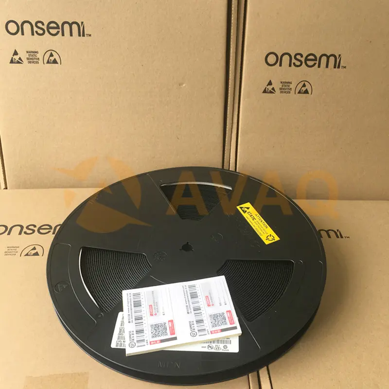
AVAQ determines and packages all devices based on electrostatic discharge (ESD) and moisture sensitivity level (MSL) protection requirements.
 Warranty

365-Day Product
Quality Guarantee
We promise to provide 365 days quality assurance service for all our products.
| Qty. | Unit Price | Ext. Price |
|---|---|---|
| 1+ | - | - |
The prices below are for reference only.