Payment Method


Advanced digital signal processing and computing capabilities for data-rich system
680-FPBGA (35x35)Manufacturer:
Mfr.Part #:
ORT8850L-2BMN680C
Datasheet:
Part Life Cycle Code:
Obsolete
Pin Count:
680
Reach Compliance Code:
not_compliant
HTS Code:
8542.39.00.01
EDA/CAD Models:
Send all BOMs to ![]() [email protected],
or fill out the form below for a quote on ORT8850L-2BMN680C. Guaranteed response within
[email protected],
or fill out the form below for a quote on ORT8850L-2BMN680C. Guaranteed response within
![]() 12hr.
12hr.
Please fill in the short form below and we will provide you the quotation immediately.
The ORT8850L-2BMN680C is a top-tier voltage regulator module defined by exceptional precision and compactness. With an input voltage range of 4.5V to 18V and an adjustable output voltage range of 0.8V to 5V, this module is suitable for a variety of power supply applications. Its maximum output current of 2A allows for effective powering of a diverse range of electronic devices and systems
| Part Life Cycle Code | Obsolete | Pin Count | 680 |
| Reach Compliance Code | not_compliant | HTS Code | 8542.39.00.01 |
| Additional Feature | SYSTEM GATES AVAILABLE UPTO 397000 | Clock Frequency-Max | 106.25 MHz |
| JESD-30 Code | S-PBGA-B680 | JESD-609 Code | e1 |
| Length | 35 mm | Moisture Sensitivity Level | 3 |
| Number of Equivalent Gates | 201000 | Number of Terminals | 680 |
| Operating Temperature-Max | 70 °C | Operating Temperature-Min | |
| Organization | 201000 GATES | Peak Reflow Temperature (Cel) | 250 |
| Programmable Logic Type | FIELD PROGRAMMABLE GATE ARRAY | Qualification Status | Not Qualified |
| Seated Height-Max | 2.51 mm | Supply Voltage-Max | 1.575 V |
| Supply Voltage-Min | 1.425 V | Supply Voltage-Nom | 1.5 V |
| Surface Mount | YES | Temperature Grade | COMMERCIAL |
| Terminal Finish | Tin/Silver/Copper (Sn96.5Ag3.0Cu0.5) | Terminal Form | BALL |
| Terminal Pitch | 1 mm | Terminal Position | BOTTOM |
| Time@Peak Reflow Temperature-Max (s) | 40 | Width | 35 mm |
| Series | ORCA® 4 | Programmabe | Not Verified |
| Number of Logic Elements/Cells | 4992 | Total RAM Bits | 75776 |
| Number of I/O | 278 | Number of Gates | 397000 |
| Voltage - Supply | 1.425V ~ 3.6V | Mounting Type | Surface Mount |
| Operating Temperature | 0°C ~ 70°C (TA) | Base Product Number | ORT8850 |
After-Sales & Settlement Related
 Payment
Payment Method


For alternative payment channels, please reach out to us at:
[email protected] Shipping & Packing
Shipping Method


AVAQ determines and packages all devices based on electrostatic discharge (ESD) and moisture sensitivity level (MSL) protection requirements.
 Warranty

365-Day Product
Quality Guarantee
We promise to provide 365 days quality assurance service for all our products.
| Qty. | Unit Price | Ext. Price |
|---|---|---|
| 1+ | - | - |
The prices below are for reference only.
LCMXO2-1200HC-4TG100I
LATTICE
1000+ $3.419
LCMXO2-1200HC-4TG100C
LATTICE
1000+ $2.604
LC4032V-75TN48C
Lattice
High Performance E2 CMOS PLD Generic Array Logic
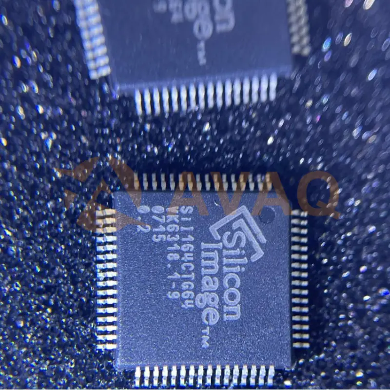
SiI164CTG64
Lattice
TQFP package Transmitter with 2 transmitters
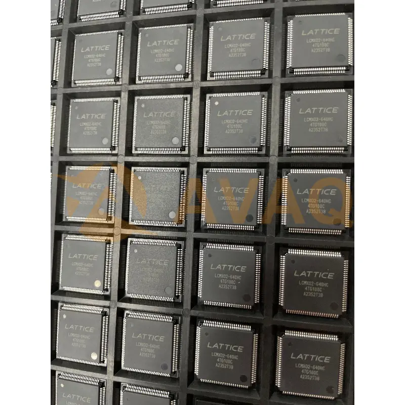
LCMXO2-640HC-4TG100C
Lattice
ROHS Programmable Logic Device (CPLDs/FPGAs) 640 80 TQFP-100(14x14) LCMXO2-640HC-4TG100C