Payment Method


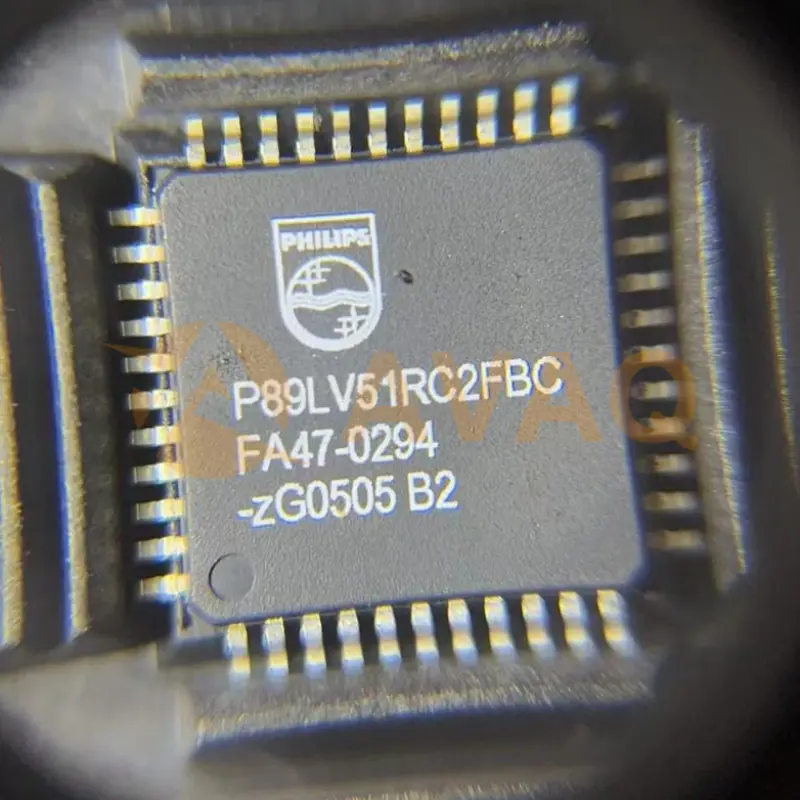
Featuring 12 CLK ISP/IAP support
TQFP-44Manufacturer:
Mfr.Part #:
P89LV51RC2FBC
Datasheet:
Part Life Cycle Code:
Obsolete
Pin Count:
44
ECCN Code:
3A991.A.2
HTS Code:
8542.31.00.01
EDA/CAD Models:
Send all BOMs to ![]() [email protected],
or fill out the form below for a quote on P89LV51RC2FBC. Guaranteed response within
[email protected],
or fill out the form below for a quote on P89LV51RC2FBC. Guaranteed response within
![]() 12hr.
12hr.
Please fill in the short form below and we will provide you the quotation immediately.
One of the standout features of the P89LV51RC2FBC is its support for various communication protocols like UART, SPI, and I2C. This flexibility makes it a breeze to connect and communicate with other devices, opening up a world of possibilities for your project. Plus, with built-in timers/counters and PWM outputs, this microcontroller is perfectly suited for applications that require precise timing control or analog device interfacing
| Source Content uid | P89LV51RC2FBC | Part Life Cycle Code | Obsolete |
| Pin Count | 44 | Reach Compliance Code | |
| ECCN Code | 3A991.A.2 | HTS Code | 8542.31.00.01 |
| Has ADC | NO | Address Bus Width | 16 |
| Bit Size | 8 | CPU Family | 8051 |
| Clock Frequency-Max | 33 MHz | DAC Channels | NO |
| DMA Channels | NO | External Data Bus Width | 8 |
| JESD-30 Code | S-PQFP-G44 | Length | 10 mm |
| Moisture Sensitivity Level | 3 | Number of I/O Lines | 32 |
| Number of Terminals | 44 | Operating Temperature-Max | 85 °C |
| Operating Temperature-Min | -40 °C | PWM Channels | YES |
| Qualification Status | Not Qualified | RAM (bytes) | 1024 |
| ROM (words) | 32768 | ROM Programmability | FLASH |
| Seated Height-Max | 1.2 mm | Speed | 33 MHz |
| Supply Current-Max | 30 mA | Supply Voltage-Max | 3.6 V |
| Supply Voltage-Min | 2.7 V | Supply Voltage-Nom | 3 V |
| Surface Mount | YES | Technology | CMOS |
| Temperature Grade | INDUSTRIAL | Terminal Form | GULL WING |
| Terminal Pitch | 0.8 mm | Terminal Position | QUAD |
| Width | 10 mm | uPs/uCs/Peripheral ICs Type | MICROCONTROLLER |
After-Sales & Settlement Related
 Payment
Payment Method


For alternative payment channels, please reach out to us at:
[email protected] Shipping & Packing
Shipping Method


AVAQ determines and packages all devices based on electrostatic discharge (ESD) and moisture sensitivity level (MSL) protection requirements.
 Warranty

365-Day Product
Quality Guarantee
We promise to provide 365 days quality assurance service for all our products.
| Qty. | Unit Price | Ext. Price |
|---|---|---|
| 1+ | - | - |
The prices below are for reference only.
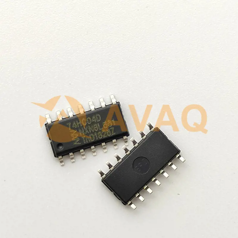
74HC04D
Toshiba
5000+ $0.072
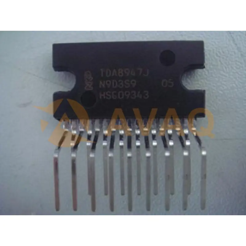
TDA8947J
NXP
Audio Amplifiers 3/4 CHANNEL AUDIO AMPLIFIER
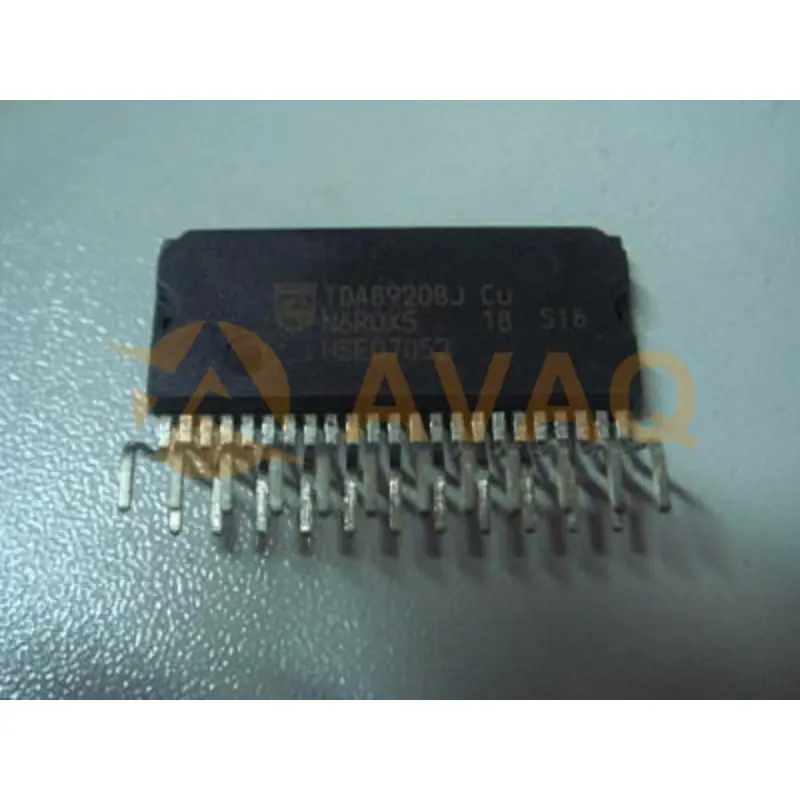
TDA8920BJ
Nxp
Experience crystal-clear sound quality and robust power handling with this efficient Class D amplifier
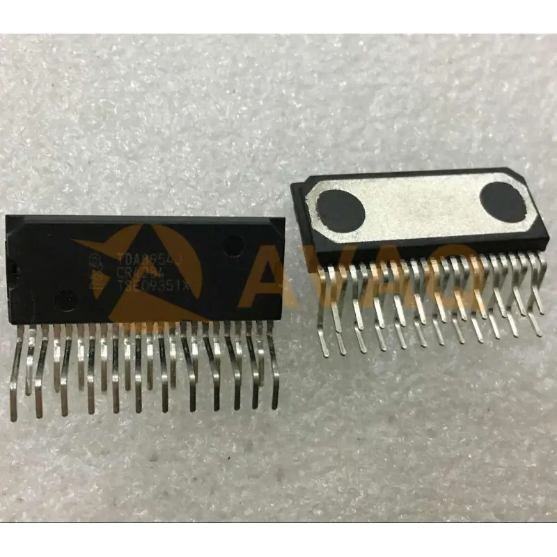
TDA8954J
Nxp
Plastic SOT411-1 PZFM23 audio amplifier
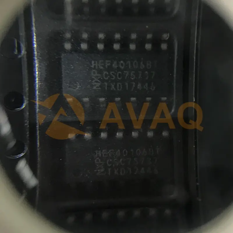
HEF40106BT
Nexperia
Inverter Schmitt Trigger 6-Element CMOS 14-Pin SO
