Payment Method


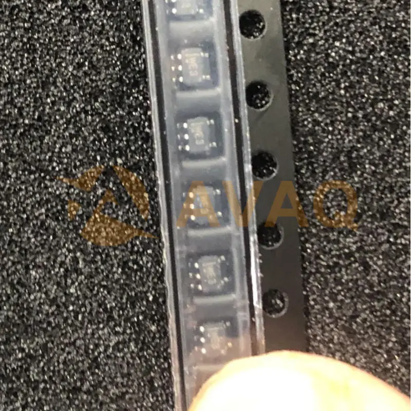
The SN74LV1T08 is a single 2-input AND gate with reduced input thresholds to support voltage translation applications.
SC70-5Manufacturer:
Mfr.Part #:
SN74LV1T08DCKR
Datasheet:
Technology Family:
LV1T
Bits (#):
1
High Input Voltage (min) (V):
1
High Input Voltage (max) (V):
5.5
EDA/CAD Models:
All bill of materials (BOM) can be sent via email to ![]() [email protected],
or fill below form to Quote for SN74LV1T08DCKR, guaranteed quotes back within
[email protected],
or fill below form to Quote for SN74LV1T08DCKR, guaranteed quotes back within
![]() 12hr.
12hr.
Please fill in the short form below and we will provide you the quotation immediately.
The SN74LV1T08DCKR is a single 2-input AND gate specifically designed for voltage translation applications. It features reduced input thresholds to support a wide range of VCC voltages, including 5.0V, 3.3V, 2.5V, and 1.8V, making it suitable for use in telecom, portable devices, servers, PCs, and notebooks. With an operating range of 1.8V to 5.5V, this CMOS logic level shifter facilitates both up and down translation scenarios, providing flexibility in various circuit designs. The logic output is referenced to VCC, and the output drive adapts to the VCC voltage level, ensuring optimal performance for different power supply configurations. Packaged in a compact SC-70 (DCK) form factor measuring 2.00mm x 2.1mm with a height of 1.25mm, the SN74LV1T08DCKR is well-suited for space-constrained applications. It is characterized for operation up to 50MHz at 3.3V VCC and has a wide operating temperature range of -40°C to 125°C, making it suitable for use in challenging environmental conditions. With its versatile features and robust design, the SN74LV1T08DCKR is an ideal choice for voltage translation and logic gate applications across various industries
The SN74LV1T08DCKR is suitable for applications such as logic level translation, bus buffering, and signal conditioning. It can also be used in automotive, industrial, and consumer applications.
| Technology family | LV1T | Bits (#) | 1 |
| High input voltage (min) (V) | 1 | High input voltage (max) (V) | 5.5 |
| Vout (min) (V) | 1.65 | Vout (max) (V) | 5.5 |
| Data rate (max) (MBps) | 100 | IOH (max) (mA) | -8 |
| IOL (max) (mA) | 8 | Supply current (max) (µA) | 10 |
| Features | Over-voltage tolerant inputs, Single supply | Input type | TTL-Compatible CMOS |
| Output type | Balanced CMOS, Push-Pull | Operating temperature range (°C) | -40 to 125 |
After-Sales & Settlement Related
 Payment
Payment Method


For alternative payment channels, please reach out to us at:
[email protected] Shipping & Packing
Shipping Method


AVAQ determines and packages all devices based on electrostatic discharge (ESD) and moisture sensitivity level (MSL) protection requirements.
 Warranty

365-Day Product
Quality Guarantee
We promise to provide 365 days quality assurance service for all our products.
| Qty. | Unit Price | Ext. Price |
|---|---|---|
| 1+ | - | - |
The prices below are for reference only.
