Payment Method


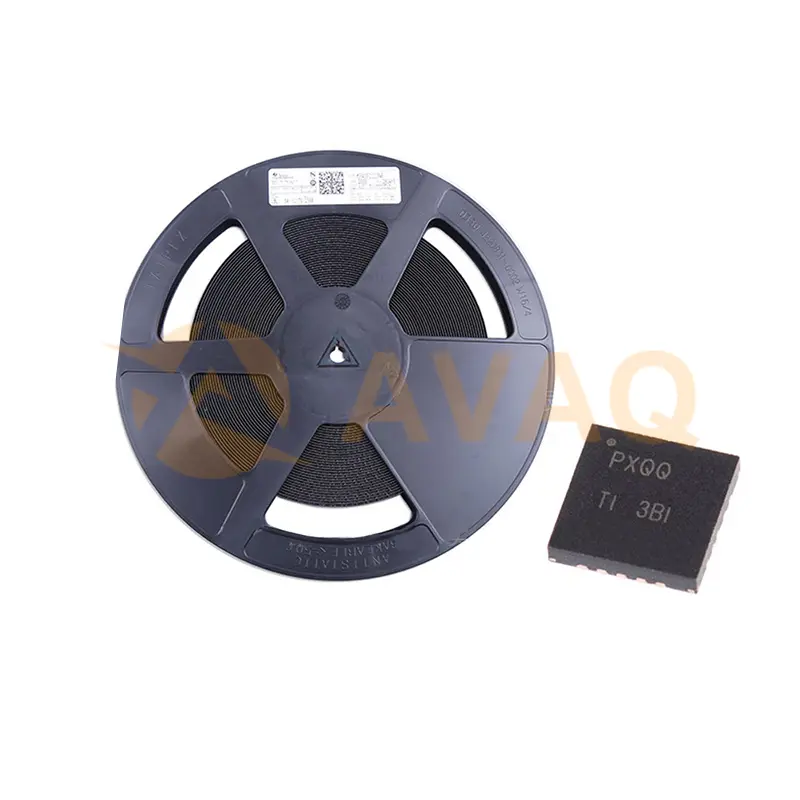
LVDS Interface IC Quad LVDS Receiver 20-LCCC -55 to 125
LCCManufacturer:
Mfr.Part #:
SNJ55LVDS32FK
Datasheet:
Function:
Receiver
Protocols:
LVDS
Number Of Transmitters:
0
Number Of Receivers:
4
EDA/CAD Models:
All bill of materials (BOM) can be sent via email to ![]() [email protected],
or fill below form to Quote for SNJ55LVDS32FK, guaranteed quotes back within
[email protected],
or fill below form to Quote for SNJ55LVDS32FK, guaranteed quotes back within
![]() 12hr.
12hr.
Please fill in the short form below and we will provide you the quotation immediately.
The SN55LVDS32, SN65LVDS32, SN65LVDS3486, and SN65LVDS9637 devices are differential line receivers that implement the electrical characteristics of low-voltage differential signaling (LVDS). This signaling technique lowers the output voltage levels of 5-V differential standard levels (such as EIA/TIA-422B) to reduce the power, increase the switching speeds, and allow operation with a 3.3-V supply rail. Any of the differential receivers provides a valid logical output state with a ±100-mV differential input voltage within the input common-mode voltage range. The input common-mode voltage range allows 1 V of ground potential difference between two LVDS nodes.
The intended application of these devices and signaling technique is both point-to-point and multidrop (one driver and multiple receivers) data transmission over controlled impedance media of approximately 100 Ω. The transmission media may be printed-circuit board traces, backplanes, or cables. The ultimate rate and distance of data transfer depends on the attenuation characteristics of the media and the noise coupling to the environment.
The SN65LVDS32, SN65LVDS3486, and SN65LVDS9637 devices are characterized for operation from –40°C to 85°C. The SN55LVDS32 device is characterized for operation from –55°C to 125°C.


| Function | Receiver | Protocols | LVDS |
| Number of transmitters | 0 | Number of receivers | 4 |
| Supply voltage (V) | 3.3 | Signaling rate (MBits) | 100 |
| Input signal | LVDS | Output signal | LVTTL |
| Rating | Military | Operating temperature range (°C) | -55 to 125 |
After-Sales & Settlement Related
 Payment
Payment Method


For alternative payment channels, please reach out to us at:
[email protected] Shipping & Packing
Shipping Method


AVAQ determines and packages all devices based on electrostatic discharge (ESD) and moisture sensitivity level (MSL) protection requirements.
 Warranty

365-Day Product
Quality Guarantee
We promise to provide 365 days quality assurance service for all our products.
| Qty. | Unit Price | Ext. Price |
|---|---|---|
| 1+ | - | - |
The prices below are for reference only.