Payment Method


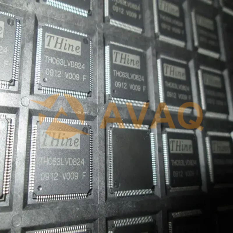
Line Driver/Receiver, PQFP100
QFP-100Manufacturer:
THINE ELECTRONICS INC
Mfr.Part #:
THC63LVD824
Datasheet:
Part Life Cycle Code:
Contact Manufacturer
Reach Compliance Code:
compliant
ECCN Code:
EAR99
HTS Code:
8542.39.00.01
EDA/CAD Models:
Please fill in the short form below and we will provide you the quotation immediately.
| Part Life Cycle Code | Contact Manufacturer | Reach Compliance Code | compliant |
| ECCN Code | EAR99 | HTS Code | 8542.39.00.01 |
| JESD-30 Code | S-PQFP-G100 | JESD-609 Code | e6 |
| Moisture Sensitivity Level | 3 | Number of Terminals | 100 |
| Operating Temperature-Max | 70 °C | Operating Temperature-Min | -10 °C |
| Power Supplies | 3.3 V | Qualification Status | Not Qualified |
| Receive Delay-Max | Supply Current-Max | 173 mA | |
| Supply Voltage-Nom | 3.3 V | Surface Mount | YES |
| Temperature Grade | COMMERCIAL | Terminal Finish | Tin/Bismuth (Sn/Bi) |
| Terminal Form | GULL WING | Terminal Pitch | 0.5 mm |
| Terminal Position | QUAD |
After-Sales & Settlement Related
 Payment
Payment Method


For alternative payment channels, please reach out to us at:
[email protected] Shipping & Packing
Shipping Method


AVAQ determines and packages all devices based on electrostatic discharge (ESD) and moisture sensitivity level (MSL) protection requirements.
 Warranty

365-Day Product
Quality Guarantee
We promise to provide 365 days quality assurance service for all our products.
| Qty. | Unit Price | Ext. Price |
|---|---|---|
| 1+ | - | - |
The prices below are for reference only.
All bill of materials (BOM) can be sent via email to ![]() [email protected],
or fill below form to Quote for THC63LVD824, guaranteed quotes back within
[email protected],
or fill below form to Quote for THC63LVD824, guaranteed quotes back within
![]() 12hr.
12hr.
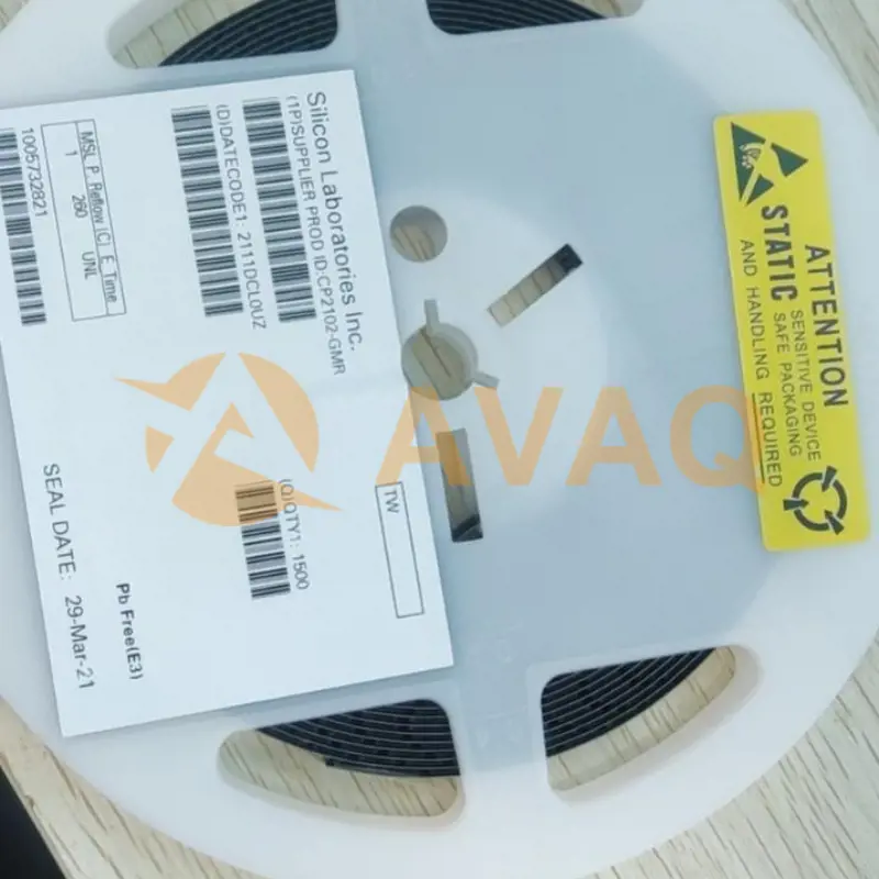
CP2102
Silicon Laboratories
Integrate seamlessly into your design with our reliable interface I
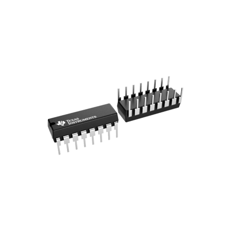
MAX232
Texas Instruments
This V device features bps data transfer rates and robust ESD protection
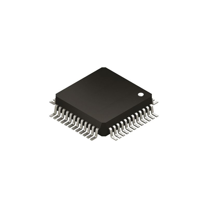
W5500
Wiznet
With its comprehensive set of protocols and interfaces, this IC streamlines network development and deploymen
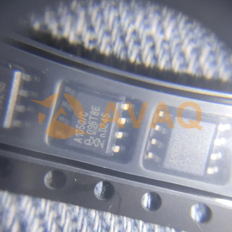
TJA1050
Nxp
Robust and reliable high-speed communication solution for demanding application

RTL2832U
Realtek
High-performance demodulation for DVB-T signals, plug-and-play via US
