Payment Method


A versatile FPGA device designed to accelerate complex digital signal processing tasks efficientl
CQFPManufacturer:
ACTEL CORP
Mfr.Part #:
A1280A-1CQ172M
Datasheet:
Part Life Cycle Code:
Transferred
Reach Compliance Code:
compliant
Additional Feature:
MAX 140 I/OS
Clock Frequency-Max:
60 MHz
EDA/CAD Models:
Send all BOMs to ![]() [email protected],
or fill out the form below for a quote on A1280A-1CQ172M. Guaranteed response within
[email protected],
or fill out the form below for a quote on A1280A-1CQ172M. Guaranteed response within
![]() 12hr.
12hr.
Please fill in the short form below and we will provide you the quotation immediately.
Intel's A1280A-1CQ172M represents the pinnacle of microprocessor technology, engineered for unparalleled performance and power efficiency. As part of the Cyclone IV series, this processor boasts a clock frequency of 172 MHz and utilizes a 28nm process technology, ensuring top-notch reliability and speed. Its innovative configurable logic block architecture empowers users with the ability to design custom logic functions, while integrated memory blocks and numerous input/output pins facilitate seamless data management and connectivity with external devices. From industrial automation to telecommunications and automotive systems, A1280A-1CQ172M is the go-to choice for applications that demand superior computational capabilities and prolonged battery life
| Part Life Cycle Code | Transferred | Reach Compliance Code | compliant |
| Additional Feature | MAX 140 I/OS | Clock Frequency-Max | 60 MHz |
| Combinatorial Delay of a CLB-Max | 4.3 ns | JESD-30 Code | S-CQFP-F172 |
| JESD-609 Code | e0 | Length | 29.972 mm |
| Number of CLBs | 1232 | Number of Equivalent Gates | 8000 |
| Number of Inputs | 140 | Number of Logic Cells | 1232 |
| Number of Outputs | 140 | Number of Terminals | 172 |
| Operating Temperature-Max | 125 °C | Operating Temperature-Min | -55 °C |
| Organization | 1232 CLBS, 8000 GATES | Peak Reflow Temperature (Cel) | 225 |
| Power Supplies | 5 V | Programmable Logic Type | FIELD PROGRAMMABLE GATE ARRAY |
| Qualification Status | Not Qualified | Seated Height-Max | 2.9464 mm |
| Supply Voltage-Max | 5.5 V | Supply Voltage-Min | 4.5 V |
| Supply Voltage-Nom | 5 V | Surface Mount | YES |
| Technology | CMOS | Temperature Grade | MILITARY |
| Terminal Finish | TIN LEAD | Terminal Form | FLAT |
| Terminal Pitch | 0.635 mm | Terminal Position | QUAD |
| Width | 29.972 mm |
After-Sales & Settlement Related
 Payment
Payment Method


For alternative payment channels, please reach out to us at:
[email protected] Shipping & Packing
Shipping Method


AVAQ determines and packages all devices based on electrostatic discharge (ESD) and moisture sensitivity level (MSL) protection requirements.
 Warranty

365-Day Product
Quality Guarantee
We promise to provide 365 days quality assurance service for all our products.
| Qty. | Unit Price | Ext. Price |
|---|---|---|
| 1+ | - | - |
The prices below are for reference only.
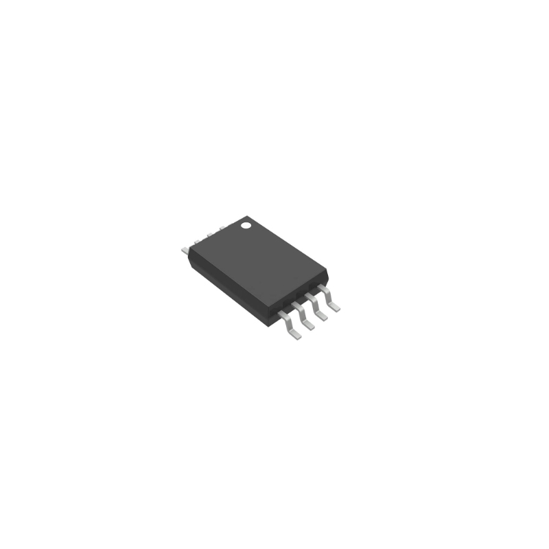
NE555
Texas Instruments
100kHz operation frequency with low power consumption for long-lasting performance
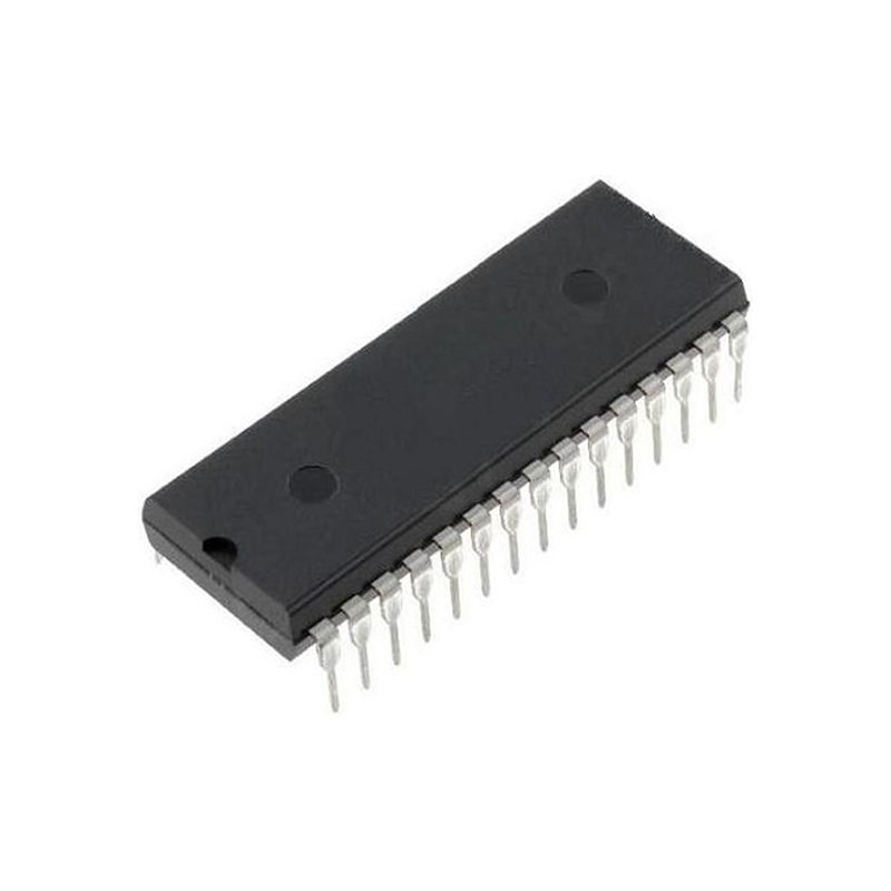
CD4017
Onsemi
Compact digital counter for precision measurement application

74LS04
Onsemi
High-quality die for professional use only, unsurfaced and untested
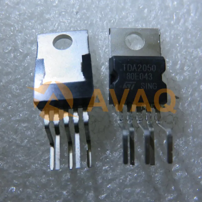
TDA2050
Stmicroelectronics
Effortlessly drives your speakers with crystal-clear sound and robust power
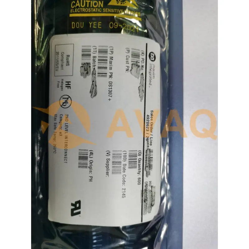
DS1307+
Analog Devices
I2C DIP-8 Real-time Clocks (RTC) ROHS