Payment Method


Small, versatile FPGA
TQFP-100Manufacturer:
Mfr.Part #:
LCMXO2-1200HC-4TG100CR1
Datasheet:
Part Life Cycle Code:
Obsolete
Pin Count:
100
HTS Code:
8542.39.00.01
Clock Frequency-Max:
133 MHz
EDA/CAD Models:
Send all BOMs to ![]() [email protected],
or fill out the form below for a quote on LCMXO2-1200HC-4TG100CR1. Guaranteed response within
[email protected],
or fill out the form below for a quote on LCMXO2-1200HC-4TG100CR1. Guaranteed response within
![]() 12hr.
12hr.
Please fill in the short form below and we will provide you the quotation immediately.
Designed for space-constrained applications, the LCMXO2-1200HC-4TG100CR1 comes in a compact 100-pin TQFP package. Its built-in security features ensure the protection of design IP and data, providing peace of mind for users. Additionally, the device's support for low-power operation makes it an ideal choice for battery-powered applications, offering energy efficiency without compromising on performance
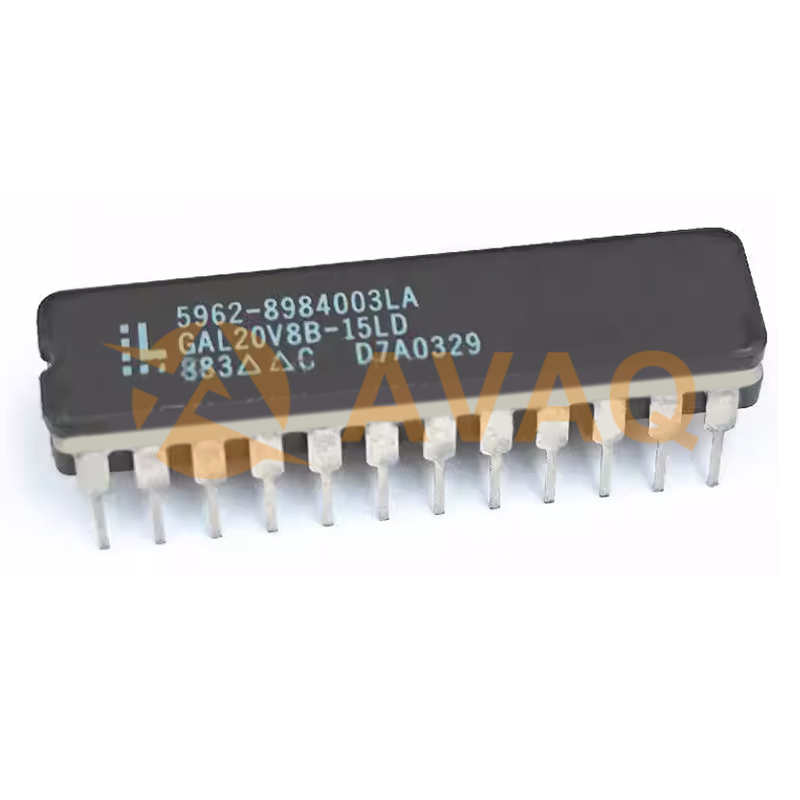
| Part Life Cycle Code | Obsolete | Pin Count | 100 |
| Reach Compliance Code | HTS Code | 8542.39.00.01 | |
| Clock Frequency-Max | 133 MHz | JESD-30 Code | S-PQFP-G100 |
| JESD-609 Code | e3 | Moisture Sensitivity Level | 3 |
| Number of Inputs | 80 | Number of Logic Cells | 1280 |
| Number of Outputs | 80 | Number of Terminals | 100 |
| Operating Temperature-Max | 85 °C | Operating Temperature-Min | |
| Peak Reflow Temperature (Cel) | 260 | Power Supplies | 2.5/3.3 V |
| Programmable Logic Type | FIELD PROGRAMMABLE GATE ARRAY | Qualification Status | Not Qualified |
| Supply Voltage-Max | 3.465 V | Supply Voltage-Min | 2.375 V |
| Supply Voltage-Nom | 2.5 V | Surface Mount | YES |
| Technology | CMOS | Temperature Grade | OTHER |
| Terminal Finish | Matte Tin (Sn) | Terminal Form | GULL WING |
| Terminal Pitch | 0.5 mm | Terminal Position | QUAD |
| Time@Peak Reflow Temperature-Max (s) | 30 |
After-Sales & Settlement Related
 Payment
Payment Method


For alternative payment channels, please reach out to us at:
[email protected] Shipping & Packing
Shipping Method


AVAQ determines and packages all devices based on electrostatic discharge (ESD) and moisture sensitivity level (MSL) protection requirements.
 Warranty

365-Day Product
Quality Guarantee
We promise to provide 365 days quality assurance service for all our products.
| Qty. | Unit Price | Ext. Price |
|---|---|---|
| 1+ | - | - |
The prices below are for reference only.
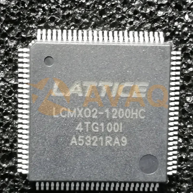
LCMXO2-1200HC-4TG100I
LATTICE
1000+ $3.419
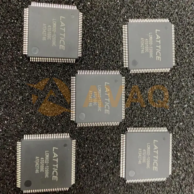
LCMXO2-1200HC-4TG100C
LATTICE
1000+ $2.604
LC4032V-75TN48C
Lattice
High Performance E2 CMOS PLD Generic Array Logic
SiI164CTG64
Lattice
TQFP package Transmitter with 2 transmitters
LCMXO2-640HC-4TG100C
Lattice
ROHS Programmable Logic Device (CPLDs/FPGAs) 640 80 TQFP-100(14x14) LCMXO2-640HC-4TG100C