Payment Method


Level Cell NAND Flash
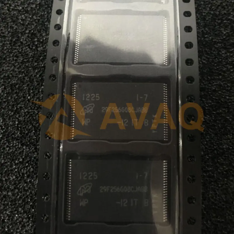
48-TSOP IManufacturer:
Micron Technology Inc.
Mfr.Part #:
MT29F256G08CJABBWP-12IT:B
Datasheet:
Part Life Cycle Code:
Obsolete
ECCN Code:
EAR99
HTS Code:
8542.32.00.51
Memory IC Type:
FLASH
EDA/CAD Models:
All bill of materials (BOM) can be sent via email to ![]() [email protected],
or fill below form to Quote for MT29F256G08CJABBWP-12IT:B, guaranteed quotes back within
[email protected],
or fill below form to Quote for MT29F256G08CJABBWP-12IT:B, guaranteed quotes back within
![]() 12hr.
12hr.
Please fill in the short form below and we will provide you the quotation immediately.
Featuring MLC technology, the MT29F256G08CJABBWP-12IT:B strikes the perfect balance between performance and affordability. Its multi-level cell array ensures reliable data retention and endurance, making it ideal for applications that require consistent read and write operations. With built-in error correction and wear-leveling mechanisms, you can trust that your data will remain secure and accessible. Whether you're a casual user or a tech enthusiast, this NAND flash memory device is a reliable choice for all your storage needs
| Part Life Cycle Code | Obsolete | Reach Compliance Code | |
| ECCN Code | EAR99 | HTS Code | 8542.32.00.51 |
| Memory IC Type | FLASH | Programming Voltage | 3.3 V |
| Type | MLC NAND TYPE | Programmabe | Not Verified |
| Memory Type | Non-Volatile | Memory Format | FLASH |
| Technology | FLASH - NAND (MLC) | Memory Size | 256Gbit |
| Memory Organization | 32G x 8 | Memory Interface | Parallel |
| Clock Frequency | 83 MHz | Voltage - Supply | 2.7V ~ 3.6V |
| Operating Temperature | -40°C ~ 85°C (TA) | Mounting Type | Surface Mount |
| Base Product Number | MT29F256G08 |
After-Sales & Settlement Related
 Payment
Payment Method


For alternative payment channels, please reach out to us at:
[email protected] Shipping & Packing
Shipping Method


AVAQ determines and packages all devices based on electrostatic discharge (ESD) and moisture sensitivity level (MSL) protection requirements.
 Warranty

365-Day Product
Quality Guarantee
We promise to provide 365 days quality assurance service for all our products.
| Qty. | Unit Price | Ext. Price |
|---|---|---|
| 1+ | - | - |
The prices below are for reference only.
