Payment Method


Flash memory with a capacity of 256 megabits organized in an 8-bit configuration with a fast access time of 25 nanoseconds
63-VFBGA (10.5x13)Manufacturer:
Micron Technology Inc.
Mfr.Part #:
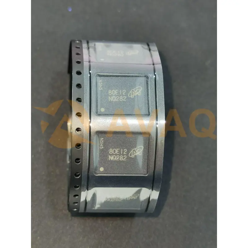
MT29F2G08ABBEAHC-IT:E
Datasheet:
Programmabe:
Verified
Memory Type:
Non-Volatile
Memory Format:
FLASH
Technology:
FLASH - NAND
EDA/CAD Models:
Send all BOMs to ![]() [email protected],
or fill out the form below for a quote on MT29F2G08ABBEAHC-IT:E. Guaranteed response within
[email protected],
or fill out the form below for a quote on MT29F2G08ABBEAHC-IT:E. Guaranteed response within
![]() 12hr.
12hr.
Please fill in the short form below and we will provide you the quotation immediately.
In terms of reliability, the MT29F2G08ABBEAHC-IT:E is equipped with built-in error correction and wear-leveling algorithms, ensuring data integrity and longevity. It also offers support for features like bad block management, data protection, and secure erase functions, providing enhanced security and peace of mind for users who prioritize the safety of their data
| Programmabe | Verified | Memory Type | Non-Volatile |
| Memory Format | FLASH | Technology | FLASH - NAND |
| Memory Size | 2Gbit | Memory Organization | 256M x 8 |
| Memory Interface | Parallel | Clock Frequency | - |
| Write Cycle Time - Word, Page | - | Access Time | - |
| Voltage - Supply | 1.7V ~ 1.95V | Operating Temperature | -40°C ~ 85°C (TA) |
| Mounting Type | Surface Mount |
After-Sales & Settlement Related
 Payment
Payment Method


For alternative payment channels, please reach out to us at:
[email protected] Shipping & Packing
Shipping Method


AVAQ determines and packages all devices based on electrostatic discharge (ESD) and moisture sensitivity level (MSL) protection requirements.
 Warranty

365-Day Product
Quality Guarantee
We promise to provide 365 days quality assurance service for all our products.
| Qty. | Unit Price | Ext. Price |
|---|---|---|
| 1+ | - | - |
The prices below are for reference only.
