Payment Method


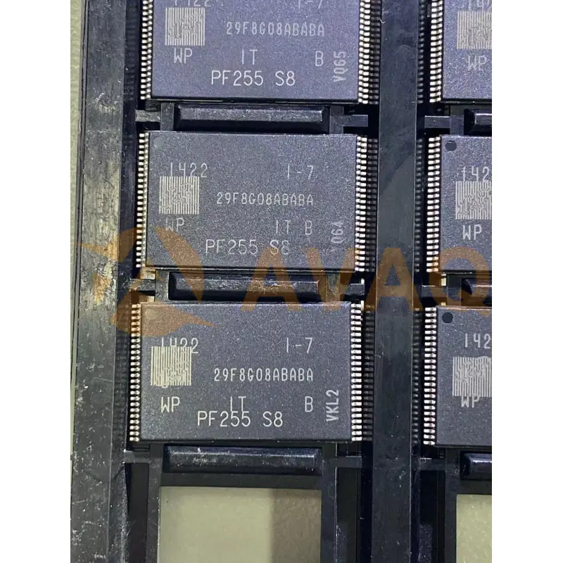
8G NAND Flash SLC TSOP
TSOP-48Manufacturer:
Micron Technology Inc.
Mfr.Part #:
MT29F8G08ABABAWP-IT:B TR
Datasheet:
Programmabe:
Verified
Memory Type:
Non-Volatile
Memory Format:
FLASH
Technology:
FLASH - NAND
EDA/CAD Models:
Send all BOMs to ![]() [email protected],
or fill out the form below for a quote on MT29F8G08ABABAWP-IT:B TR. Guaranteed response within
[email protected],
or fill out the form below for a quote on MT29F8G08ABABAWP-IT:B TR. Guaranteed response within
![]() 12hr.
12hr.
Please fill in the short form below and we will provide you the quotation immediately.
Unleash the potential of your devices with the MT29F8G08ABABAWP-IT:B TR, a NAND flash memory chip that embodies innovation and performance. Micron Technology's expertise shines through in this chip, offering a generous 8 gigabytes of storage capacity and a seamless parallel interface for lightning-fast data access. Whether used in consumer electronics or industrial equipment, this chip's robust features, including error correction and wide temperature tolerance, ensure optimal performance in any setting. Embrace the future of storage technology with the MT29F8G08ABABAWP-IT:B TR, where efficiency and reliability converge to elevate your user experience
| Programmabe | Verified | Memory Type | Non-Volatile |
| Memory Format | FLASH | Technology | FLASH - NAND |
| Memory Size | 8Gbit | Memory Organization | 1G x 8 |
| Memory Interface | Parallel | Clock Frequency | - |
| Write Cycle Time - Word, Page | - | Access Time | - |
| Voltage - Supply | 2.7V ~ 3.6V | Operating Temperature | -40°C ~ 85°C (TA) |
| Mounting Type | Surface Mount |
After-Sales & Settlement Related
 Payment
Payment Method


For alternative payment channels, please reach out to us at:
[email protected] Shipping & Packing
Shipping Method


AVAQ determines and packages all devices based on electrostatic discharge (ESD) and moisture sensitivity level (MSL) protection requirements.
 Warranty

365-Day Product
Quality Guarantee
We promise to provide 365 days quality assurance service for all our products.
| Qty. | Unit Price | Ext. Price |
|---|---|---|
| 1+ | - | - |
The prices below are for reference only.
