Payment Method


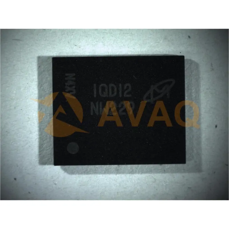
NAND Flash, SLC NAND Flash, 8Gb, 3.3V, 63-ball VFBGA, RoHS
63-VFBGA (9x11)Manufacturer:
Micron Technology Inc.
Mfr.Part #:
MT29F8G16ADADAH4-IT:D
Datasheet:
Programmabe:
Not Verified
Memory Type:
Non-Volatile
Memory Format:
FLASH
Technology:
FLASH - NAND
EDA/CAD Models:
Send all BOMs to ![]() [email protected],
or fill out the form below for a quote on MT29F8G16ADADAH4-IT:D. Guaranteed response within
[email protected],
or fill out the form below for a quote on MT29F8G16ADADAH4-IT:D. Guaranteed response within
![]() 12hr.
12hr.
Please fill in the short form below and we will provide you the quotation immediately.
As a RoHS-compliant product, the MT29F8G16ADADAH4-IT:D meets strict environmental standards, making it a sustainable choice for environmentally-conscious consumers. Its compact design and high-speed performance make it suitable for a variety of industrial, automotive, and consumer electronics applications
| Programmabe | Not Verified | Memory Type | Non-Volatile |
| Memory Format | FLASH | Technology | FLASH - NAND |
| Memory Size | 8Gbit | Memory Organization | 512M x 16 |
| Memory Interface | Parallel | Clock Frequency | - |
| Write Cycle Time - Word, Page | - | Access Time | - |
| Voltage - Supply | 2.7V ~ 3.6V | Operating Temperature | -40°C ~ 85°C (TA) |
| Mounting Type | Surface Mount |
After-Sales & Settlement Related
 Payment
Payment Method


For alternative payment channels, please reach out to us at:
[email protected] Shipping & Packing
Shipping Method


AVAQ determines and packages all devices based on electrostatic discharge (ESD) and moisture sensitivity level (MSL) protection requirements.
 Warranty

365-Day Product
Quality Guarantee
We promise to provide 365 days quality assurance service for all our products.
| Qty. | Unit Price | Ext. Price |
|---|---|---|
| 1+ | - | - |
The prices below are for reference only.
