Payment Method


Active high enable simplifies circuit desi
SOT-SC70 (DCK)-5Manufacturer:
Mfr.Part #:
SN74LV1T126DCKR
Datasheet:
Technology Family:
LV1T
Applications:
GPIO, I2S, UART
Bits (#):
1
Configuration:
1 Ch A to B 0 Ch B to A
EDA/CAD Models:
All bill of materials (BOM) can be sent via email to ![]() [email protected],
or fill below form to Quote for SN74LV1T126DCKR, guaranteed quotes back within
[email protected],
or fill below form to Quote for SN74LV1T126DCKR, guaranteed quotes back within
![]() 12hr.
12hr.
Please fill in the short form below and we will provide you the quotation immediately.
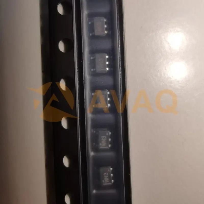
The SN74LV1T126DCKR is a single buffer gate with a 3-state output in a DCK package. It is a CMOS logic level shifter with a single-supply voltage translator supporting various voltage levels such as 5V, 3.3V, 2.5V, and 1.8V. The device has an operating range of 1.8V to 5.5V and can perform both up and down translations between different voltage levels. It has an output drive capability of 7mA at 3.3V and is characterized up to 50MHz at 3.3V VCC. The package size for SN74LV1T126DCKR is 2.00mm x 1.25mm.
| Technology family | LV1T | Applications | GPIO, I2S, UART |
| Bits (#) | 1 | Configuration | 1 Ch A to B 0 Ch B to A |
| High input voltage (min) (V) | 1 | High input voltage (max) (V) | 5.5 |
| Vout (min) (V) | 46138 | Vout (max) (V) | 5.5 |
| Data rate (max) (MBps) | 100 | IOH (max) (mA) | -8 |
| IOL (max) (mA) | -8 | Supply current (max) (µA) | 5.5 |
| Features | 4.2, 4.64 | Input type | TTL-Compatible CMOS |
| Output type | 3-State, Balanced CMOS | Rating | Catalog |
| Operating temperature range (°C) | -40 to 125 |
After-Sales & Settlement Related
 Payment
Payment Method


For alternative payment channels, please reach out to us at:
[email protected] Shipping & Packing
Shipping Method


AVAQ determines and packages all devices based on electrostatic discharge (ESD) and moisture sensitivity level (MSL) protection requirements.
 Warranty

365-Day Product
Quality Guarantee
We promise to provide 365 days quality assurance service for all our products.
| Qty. | Unit Price | Ext. Price |
|---|---|---|
| 1+ | - | - |
The prices below are for reference only.
