Payment Method


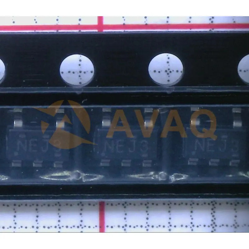
Bus Driver, LV/LV-A/LVX/H Series, 1-Func, 1-Bit, True Output, CMOS, PDSO5
SOT-23 (DBV)-5Manufacturer:
Mfr.Part #:
SN74LV1T34DBVR
Datasheet:
Technology Family:
LV1T
Applications:
GPIO
Bits (#):
1
Configuration:
1 Ch A to B 0 Ch B to A
EDA/CAD Models:
All bill of materials (BOM) can be sent via email to ![]() [email protected],
or fill below form to Quote for SN74LV1T34DBVR, guaranteed quotes back within
[email protected],
or fill below form to Quote for SN74LV1T34DBVR, guaranteed quotes back within
![]() 12hr.
12hr.
Please fill in the short form below and we will provide you the quotation immediately.
Operating within a supply voltage range of 1.6V to 5.5V, this buffer gate is suitable for various applications where signal conversion or level shifting is required. The logic IC family of SN74LV ensures reliable performance, making it a preferred choice for designers and engineers
(1)Refer to the VIH/VIL and output drive for lower VCC condition.
The SN74LV1T34DBVR is suitable for applications such as data transmission, signal buffering, and logic level conversion. It can be used in a variety of consumer electronics, automotive, and industrial applications.
| Technology family | LV1T | Applications | GPIO |
| Bits (#) | 1 | Configuration | 1 Ch A to B 0 Ch B to A |
| High input voltage (min) (V) | 1 | High input voltage (max) (V) | 5.5 |
| Vout (min) (V) | 789532 | Vout (max) (V) | 5.5 |
| Data rate (max) (MBps) | 100 | IOH (max) (mA) | -8 |
| IOL (max) (mA) | -8 | Supply current (max) (µA) | 5.5 |
| Features | 4.2, 4.64 | Input type | TTL-Compatible CMOS |
| Output type | Balanced CMOS, Push-Pull | Rating | Catalog |
| Operating temperature range (°C) | -40 to 125 |
After-Sales & Settlement Related
 Payment
Payment Method


For alternative payment channels, please reach out to us at:
[email protected] Shipping & Packing
Shipping Method


AVAQ determines and packages all devices based on electrostatic discharge (ESD) and moisture sensitivity level (MSL) protection requirements.
 Warranty

365-Day Product
Quality Guarantee
We promise to provide 365 days quality assurance service for all our products.
| Qty. | Unit Price | Ext. Price |
|---|---|---|
| 5+ | $0.188 | $0.94 |
| 50+ | $0.149 | $7.45 |
| 150+ | $0.132 | $19.80 |
| 500+ | $0.111 | $55.50 |
| 3000+ | $0.103 | $309.00 |
| 6000+ | $0.097 | $582.00 |
The prices below are for reference only.
