Payment Method


Ultra-compact IC enables high-density power application
HVSSOP (DGN)-8Manufacturer:
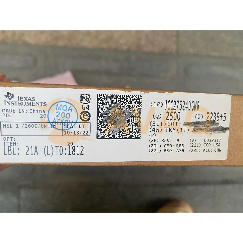
Mfr.Part #:
UCC27524DGNR
Datasheet:
Number Of Channels:
2
Power Switch:
GaNFET, IGBT, MOSFET
Peak Output Current (A):
5
Input VCC (min) (V):
4.5
EDA/CAD Models:
Send all BOMs to ![]() [email protected],
or fill out the form below for a quote on UCC27524DGNR. Guaranteed response within
[email protected],
or fill out the form below for a quote on UCC27524DGNR. Guaranteed response within
![]() 12hr.
12hr.
Please fill in the short form below and we will provide you the quotation immediately.
UCC27524DGNR is a MOSFET driver with a low side configuration, designed for efficient and reliable operation. It features a peak output current of 5A, making it suitable for driving power MOSFETs in a wide range of applications. The driver operates within a supply voltage range of 4.5V to 18V, ensuring compatibility with different power supply designs. Its MSOP PowerPAD package offers a compact and space-saving solution for easy integration. With its high-performance specifications, this driver is an excellent choice for demanding applications that require precise and responsive MOSFET control
| Number of channels | 2 | Power switch | GaNFET, IGBT, MOSFET |
| Peak output current (A) | 5 | Input VCC (min) (V) | 4.5 |
| Input VCC (max) (V) | 18 | Features | Enable pin |
| Operating temperature range (°C) | -40 to 140 | Rise time (ns) | 7 |
| Fall time (ns) | 6 | Propagation delay time (µs) | 0.013 |
| Input threshold | CMOS, TTL | Channel input logic | Dual, Non-Inverting |
| Input negative voltage (V) | 0 | Rating | Catalog |
| Undervoltage lockout (typ) (V) | 4 | Driver configuration | Dual, Non-Inverting |
After-Sales & Settlement Related
 Payment
Payment Method


For alternative payment channels, please reach out to us at:
[email protected] Shipping & Packing
Shipping Method


AVAQ determines and packages all devices based on electrostatic discharge (ESD) and moisture sensitivity level (MSL) protection requirements.
 Warranty

365-Day Product
Quality Guarantee
We promise to provide 365 days quality assurance service for all our products.
| Qty. | Unit Price | Ext. Price |
|---|---|---|
| 1+ | - | - |
The prices below are for reference only.
