Payment Method


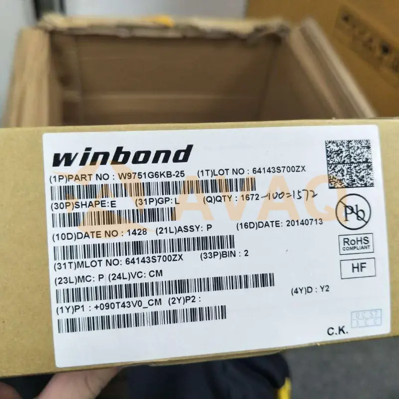
DDR2 ; 512M HZ /CL3, Lead free
FBGA84Manufacturer:
Mfr.Part #:
W9751G6JB-25
Datasheet:
ECCN (US):
EAR99
HTS:
8541.29.00.95
SVHC:
Yes
SVHC Exceeds Threshold:
Yes
EDA/CAD Models:
Please fill in the short form below and we will provide you the quotation immediately.
| ECCN (US) | EAR99 | Part Status | Active |
| HTS | 8541.29.00.95 | SVHC | Yes |
| SVHC Exceeds Threshold | Yes | Automotive | No |
| PPAP | No | Category | Power MOSFET |
| Configuration | Single Quad Drain Triple Source | Process Technology | ThunderFET |
| Channel Mode | Enhancement | Channel Type | P |
| Number of Elements per Chip | 1 | Maximum Drain Source Voltage (V) | 100 |
| Maximum Gate Source Voltage (V) | ±20 | Maximum Gate Threshold Voltage (V) | 2.6 |
| Operating Junction Temperature (°C) | -55 to 150 | Maximum Continuous Drain Current (A) | 48 |
| Maximum Gate Source Leakage Current (nA) | 100 | Maximum IDSS (uA) | 1 |
| Maximum Drain Source Resistance (mOhm) | 20@10V | Typical Gate Charge @ Vgs (nC) | [email protected]|58@10V |
| Typical Gate Charge @ 10V (nC) | 58 | Typical Gate to Drain Charge (nC) | 10.2 |
| Typical Gate to Source Charge (nC) | 12.9 | Typical Reverse Recovery Charge (nC) | 152 |
| Typical Input Capacitance @ Vds (pF) | 3395@50V | Typical Reverse Transfer Capacitance @ Vds (pF) | 55@50V |
| Minimum Gate Threshold Voltage (V) | 1.4 | Typical Output Capacitance (pF) | 910 |
| Maximum Power Dissipation (mW) | 5200 | Typical Fall Time (ns) | 15|18 |
| Typical Rise Time (ns) | 17|51 | Typical Turn-Off Delay Time (ns) | 70|38 |
| Typical Turn-On Delay Time (ns) | 15|76 | Minimum Operating Temperature (°C) | -55 |
| Maximum Operating Temperature (°C) | 150 | Packaging | Tape and Reel |
| Maximum Power Dissipation on PCB @ TC=25°C (W) | 5.2 | Maximum Pulsed Drain Current @ TC=25°C (A) | 300 |
| Maximum Junction Ambient Thermal Resistance on PCB (°C/W) | 60 | Typical Diode Forward Voltage (V) | 0.81 |
| Typical Gate Plateau Voltage (V) | 4 | Typical Reverse Recovery Time (ns) | 62 |
| Maximum Diode Forward Voltage (V) | 1.2 | Minimum Gate Resistance (Ohm) | 1 |
| Maximum Gate Resistance (Ohm) | 5.5 | Maximum Positive Gate Source Voltage (V) | 20 |
| Maximum Continuous Drain Current on PCB @ TC=25°C (A) | 11.6 | Mounting | Surface Mount |
| PCB changed | 8 | Pin Count | 8 |
After-Sales & Settlement Related
 Payment
Payment Method


For alternative payment channels, please reach out to us at:
[email protected] Shipping & Packing
Shipping Method


AVAQ determines and packages all devices based on electrostatic discharge (ESD) and moisture sensitivity level (MSL) protection requirements.
 Warranty

365-Day Product
Quality Guarantee
We promise to provide 365 days quality assurance service for all our products.
| Qty. | Unit Price | Ext. Price |
|---|---|---|
| 1+ | - | - |
The prices below are for reference only.
All bill of materials (BOM) can be sent via email to ![]() [email protected],
or fill below form to Quote for W9751G6JB-25, guaranteed quotes back within
[email protected],
or fill below form to Quote for W9751G6JB-25, guaranteed quotes back within
![]() 12hr.
12hr.
