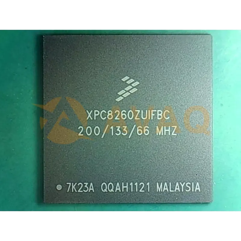
Key Features
The following list summarizes the key MPC860 features:
Embedded single-issue, 32-bit MPC8xx core (implementing the PowerPC architecture) with thirty-two 32-bit general-purpose registers (GPRs)
The core performs branch prediction with conditional prefetch, without conditional execution
4- or 8-Kbyte data cache and 4- or 16-Kbyte instruction cache (see Table 1)
16-Kbyte instruction caches are four-way, set-associative with 256 sets;
4-Kbyte instruction caches are two-way, set-associative with 128 sets.
8-Kbyte data caches are two-way, set-associative with 256 sets; 4-Kbyte data caches are two-way, set-associative with 128 sets.
Cache coherency for both instruction and data caches is maintained on 128-bit (4-word) cache blocks.
Caches are physically addressed, implement a least recently used (LRU) replacement algorithm, and are lockable on a cache block basis.
Instruction and data caches are two-way, set-associative, physically addressed, LRU replacement, and lockable on-line granularity.
MMUs with 32-entry TLB, fully associative instruction, and data TLBs
MMUs support multiple page sizes of 4, 16, and 512 Kbytes, and 8 Mbytes; 16 virtual address spaces and 16 protection groups
Advanced on-chip-emulation debug mode
Up to 32-bit data bus (dynamic bus sizing for 8, 16, and 32 bits)
32 address lines
Operates at up to 80 MHz
Memory controller (eight banks)
Contains complete dynamic RAM (DRAM) controller
Each bank can be a chip select or RASto support a DRAM bank
Up to 15 wait states programmable per memory bank
Glueless interface to DRAM, SIMMS, SRAM, EPROM, Flash EPROM, and other memory devices.
DRAM controller programmable to support most size and speed memory interfaces
Four CASlines, four WElines, one OEline
Boot chip-select available at reset (options for 8-, 16-, or 32-bit memory)
Variable block sizes (32 Kbyte to 256 Mbyte)
Selectable write protection
On-chip bus arbitration logic
General-purpose timers
Four 16-bit timers or two 32-bit timers
Gate mode can enable/disable counting
Interrupt can be masked on reference match and event capture
System integration unit (SIU)
Bus monitor
Software watchdog
Periodic interrupt timer (PIT)
Low-power stop mode
Clock synthesizer
Three parallel I/O registers with open-drain capability
Four baud-rate generators (BRGs)
Independent (can be connected to any SCC or SMC)
Allow changes during operation
Autobaud support option
Four serial communications controllers (SCCs)
Ethernet/IEEE 802.3 optional on SCC14, supporting full 10-Mbps operation (available only on specially programmed devices).
HDLC/SDLC(all channels supported at 2 Mbps)
HDLC bus (implements an HDLC-based local area network (LAN))
Asynchronous HDLC to support PPP (point-to-point protocol)
AppleTalk
Universal asynchronous receiver transmitter (UART)
Synchronous UART
Serial infrared (IrDA)
Binary synchronous communication (BISYNC)
Totally transparent (bit streams)
Totally transparent (frame based with optional cyclic redundancy check (CRC))
Two SMCs (serial management channels)
UART
Transparent
General circuit interface (GCI) controller
Can be connected to the time-division multiplexed (TDM) channels
One SPI (serial peripheral interface)
Supports master and slave modes
Supports multimaster operation on the same bus
One I2C (inter-integrated circuit) port
Supports master and slave modes
Multiple-master environment support
Time-slot assigner (TSA)
Allows SCCs and SMCs to run in multiplexed and/or non-multiplexed operation
Supports T1, CEPT, PCM highway, ISDN basic rate, ISDN primary rate, user defined
1- or 8-bit resolution
Allows independent transmit and receive routing, frame synchronization, clocking
Allows dynamic changes
Can be internally connected to six serial channels (four SCCs and two SMCs)
Parallel interface port (PIP)
Centronics interface support
Supports fast connection between compatible ports on the MPC860 or the MC68360
PCMCIA interface
Master (socket) interface, release 2.1 compliant
Supports two independent PCMCIA sockets
Eight memory or I/O windows supported
Low power support
Full onall units fully powered
Dozecore functional units disabled, except time base decrementer, PLL, memory controller, RTC, and CPM in low-power standby
Sleepall units disabled, except RTC and PIT, PLL active for fast wake up
Deep sleepall units disabled including PLL, except RTC and PIT
Power down mode all units powered down, except PLL, RTC, PIT, time base, and decrementer
Debug interface
Eight comparators: four operate on instruction address, two operate on data address, and two operate on data
Supports conditions: =<>
Each watchpoint can generate a break-point internally
3.3 V operation with 5-V TTL compatibility except EXTAL and EXTCLK
357-pin ball grid array (BGA) package


 Payment


 Shipping & Packing


 Warranty