Payment Method


1 4mA 0.8V~3.6V 1 TSSOP-5 Buffer/Driver/Transceiver ROHS
TSSOP-5Manufacturer:
Mfr.Part #:
74AUP1G07GW,125
Datasheet:
Type Number:
74AUP1G07GW
VCC (V):
0.8 - 3.6
Logic Switching Levels:
CMOS
Output Drive Capability (mA):
1.9
EDA/CAD Models:
All bill of materials (BOM) can be sent via email to ![]() [email protected],
or fill below form to Quote for 74AUP1G07GW,125, guaranteed quotes back within
[email protected],
or fill below form to Quote for 74AUP1G07GW,125, guaranteed quotes back within
![]() 12hr.
12hr.
Please fill in the short form below and we will provide you the quotation immediately.
With its comprehensive specifications and thoughtful design considerations, the 74AUP1G07GW stands out as a dependable and efficient solution for a wide range of electronic applications. Whether in consumer electronics, industrial equipment, or automotive systems, this single buffer excels in providing stable signal amplification while prioritizing power efficiency and protection. Its versatility, reliability, and low-power operation make it a valuable component for engineers seeking reliable performance in demanding environments
| Type number | 74AUP1G07GW | VCC (V) | 0.8 - 3.6 |
| Logic switching levels | CMOS | Output drive capability (mA) | 1.9 |
| fmax (MHz) | 70 | Nr of bits | 1 |
| Power dissipation considerations | ultra low | Tamb (°C) | -40~125 |
| Rth(j-a) (K/W) | 309 | Rth(j-c) (K/W) | 179 |
| Packing | SOT353-1_125 | Orderable part number | 74AUP1G07GW,125 |
| Chemical content | 74AUP1G07GW |
After-Sales & Settlement Related
 Payment
Payment Method


For alternative payment channels, please reach out to us at:
[email protected] Shipping & Packing
Shipping Method


AVAQ determines and packages all devices based on electrostatic discharge (ESD) and moisture sensitivity level (MSL) protection requirements.
 Warranty

365-Day Product
Quality Guarantee
We promise to provide 365 days quality assurance service for all our products.
| Qty. | Unit Price | Ext. Price |
|---|---|---|
| 5+ | $0.112 | $0.56 |
| 50+ | $0.092 | $4.60 |
| 150+ | $0.084 | $12.60 |
| 500+ | $0.076 | $38.00 |
| 3000+ | $0.062 | $186.00 |
| 6000+ | $0.059 | $354.00 |
The prices below are for reference only.
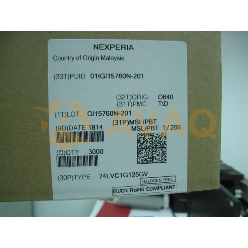
74LVC1G125GV
Nexperia
1000+ $1.033
74LVC1G125GW
Nexperia
Versatile non-inverting CMOS line driver
74LVC1G126GW
Nexperia
-state bus buffer line driver
IP4234CZ6
Nexperia
ESD TVS Diode for USB 2.0 in SOT-457 Package

74AUP1T34GW
Nexperia
Single-channel voltage level translator designed for automotive applications with a unidirectional signal flow