Payment Method


This N-Channel JFET device is designed for high frequency amplifiers and oscillators.
TO-92Manufacturer:
Mfr.Part #:
J309
Datasheet:
Technology:
Si
Mounting Style:
Through Hole
Transistor Polarity:
N-Channel
Configuration:
Single
EDA/CAD Models:
Please fill in the short form below and we will provide you the quotation immediately.
This N-Channel JFET device is designed for high frequency amplifiers and oscillators.
| Product Category | JFET | Technology | Si |
| Mounting Style | Through Hole | Transistor Polarity | N-Channel |
| Configuration | Single | Vds - Drain-Source Breakdown Voltage | 10 V |
| Vgs - Gate-Source Breakdown Voltage | - 25 V | Gate-Source Cutoff Voltage | - 4 V |
| Drain-Source Current at Vgs=0 | 30 mA | Id - Continuous Drain Current | 1 nA |
| Pd - Power Dissipation | 360 mW | Series | J309 |
| Forward Transconductance - Min | 10000 uS | Product Type | JFETs |
| Factory Pack Quantity | 1 | Subcategory | Transistors |
| Type | JFET | Unit Weight | 0.016000 oz |
After-Sales & Settlement Related
 Payment
Payment Method


For alternative payment channels, please reach out to us at:
[email protected] Shipping & Packing
Shipping Method


AVAQ determines and packages all devices based on electrostatic discharge (ESD) and moisture sensitivity level (MSL) protection requirements.
 Warranty

365-Day Product
Quality Guarantee
We promise to provide 365 days quality assurance service for all our products.
| Qty. | Unit Price | Ext. Price |
|---|---|---|
| 1+ | - | - |
The prices below are for reference only.
All bill of materials (BOM) can be sent via email to ![]() [email protected],
or fill below form to Quote for J309, guaranteed quotes back within
[email protected],
or fill below form to Quote for J309, guaranteed quotes back within
![]() 12hr.
12hr.
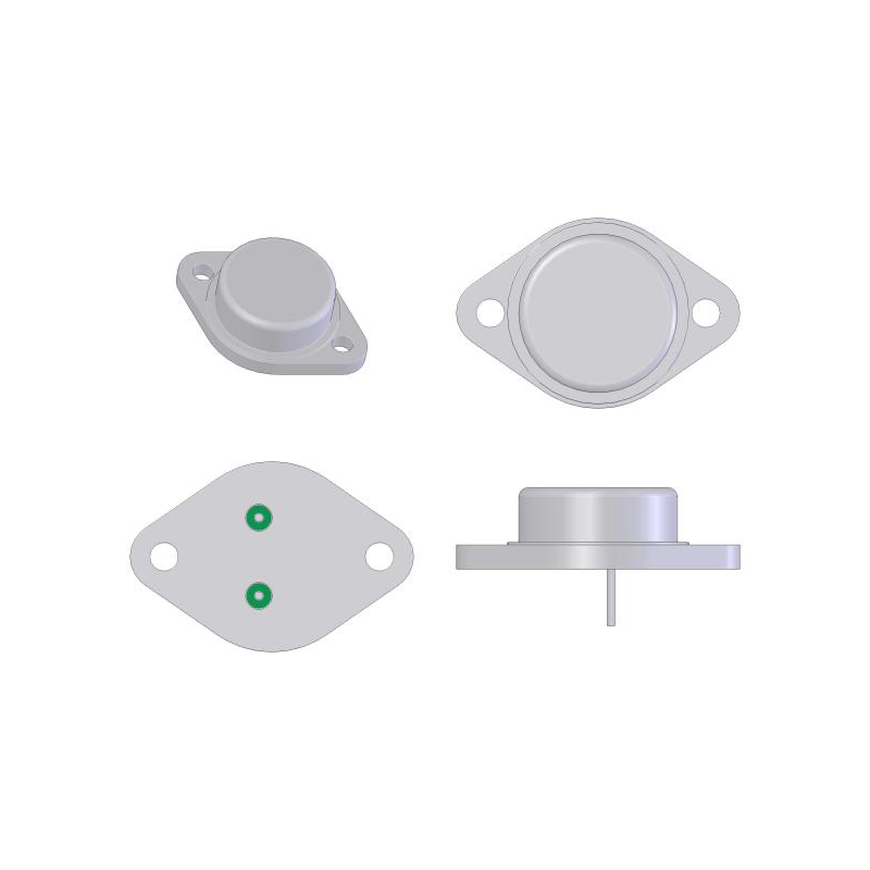
U234
InterFET
JFET JFET N-Channel(Dual) -50V Low Ciss
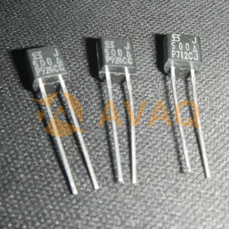
J500
InterFET
Current Regulator Diodes Current Regulator Diode 50V Low Noise

U233
InterFET
JFET JFET N-Channel(Dual) -50V Low Ciss
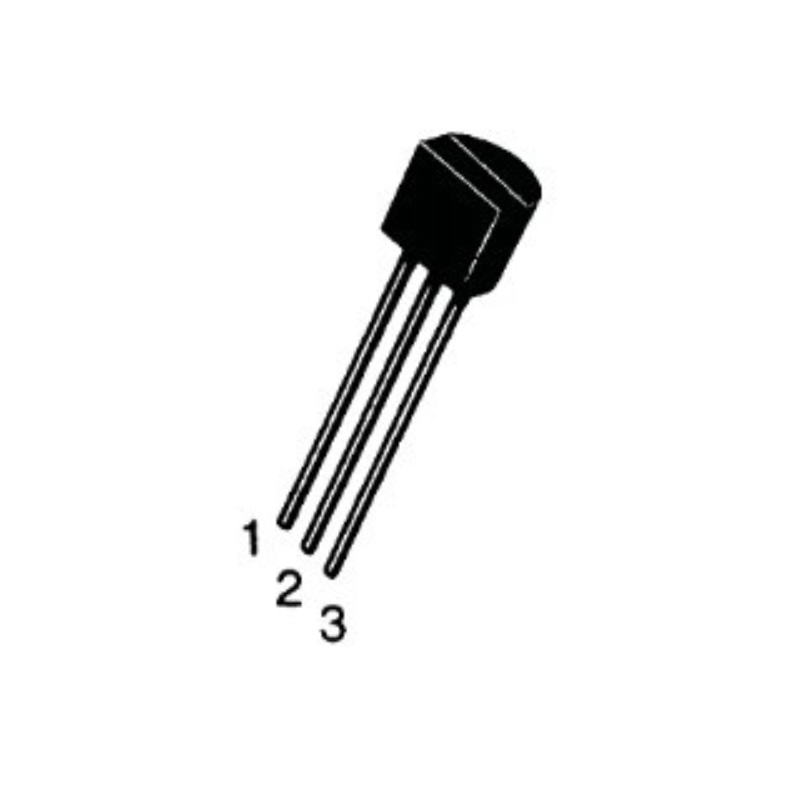
J202
InterFET
JFET N-Channel 40 V 625 mW Through Hole TO-92-3
U404
InterFET
JFET JFET N-Channel(Dual) -50V Low Ciss