Payment Method


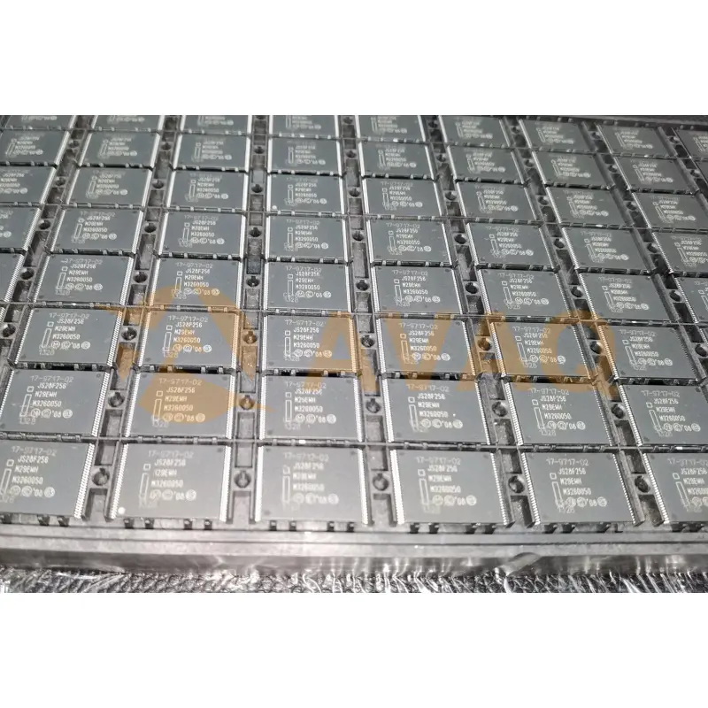
The JS28F256M29EWHA NOR flash memory device is housed in a TSOP-56 package and meets RoHS environmental standards
56-TSOPManufacturer:
Micron Technology Inc.
Mfr.Part #:
JS28F256M29EWHA
Datasheet:
Pbfree Code:
Yes
Part Life Cycle Code:
Obsolete
Pin Count:
56
Reach Compliance Code:
compliant
EDA/CAD Models:
Please fill in the short form below and we will provide you the quotation immediately.
With its comprehensive feature set and high-performance capabilities, the JS28F256M29EWHA represents a significant leap forward in NAND Flash technology. Its efficient data retrieval and storage capabilities make it a standout choice for designers and engineers looking for a reliable and high-performance memory solution. From its extended temperature range operation to its advanced wear-leveling algorithms, this chip is poised to deliver exceptional results in a wide range of applications
| Pbfree Code | Yes | Part Life Cycle Code | Obsolete |
| Pin Count | 56 | Reach Compliance Code | compliant |
| ECCN Code | EAR99 | HTS Code | 8542.32.00.51 |
| Access Time-Max | 110 ns | Alternate Memory Width | 8 |
| Command User Interface | YES | Common Flash Interface | YES |
| Data Polling | YES | JESD-30 Code | R-PDSO-G56 |
| JESD-609 Code | e3 | Length | 18.4 mm |
| Memory Density | 268435456 bit | Memory IC Type | FLASH |
| Memory Width | 16 | Number of Functions | 1 |
| Number of Sectors/Size | 256 | Number of Terminals | 56 |
| Number of Words | 16777216 words | Number of Words Code | 16000000 |
| Operating Mode | ASYNCHRONOUS | Operating Temperature-Max | 85 °C |
| Operating Temperature-Min | -40 °C | Organization | 16MX16 |
| Page Size | 16/32 words | Parallel/Serial | PARALLEL |
| Peak Reflow Temperature (Cel) | 260 | Programming Voltage | 3 V |
| Qualification Status | Not Qualified | Ready/Busy | YES |
| Seated Height-Max | 1.2 mm | Sector Size | 128K |
| Standby Current-Max | 0.00021 A | Supply Current-Max | 0.031 mA |
| Supply Voltage-Max (Vsup) | 3.6 V | Supply Voltage-Min (Vsup) | 2.7 V |
| Supply Voltage-Nom (Vsup) | 3 V | Surface Mount | YES |
| Technology | CMOS | Temperature Grade | INDUSTRIAL |
| Terminal Finish | Matte Tin (Sn) | Terminal Form | GULL WING |
| Terminal Pitch | 0.5 mm | Terminal Position | DUAL |
| Time@Peak Reflow Temperature-Max (s) | 30 | Toggle Bit | YES |
| Type | NOR TYPE | Width | 14 mm |
After-Sales & Settlement Related
 Payment
Payment Method


For alternative payment channels, please reach out to us at:
[email protected] Shipping & Packing
Shipping Method


AVAQ determines and packages all devices based on electrostatic discharge (ESD) and moisture sensitivity level (MSL) protection requirements.
 Warranty

365-Day Product
Quality Guarantee
We promise to provide 365 days quality assurance service for all our products.
| Qty. | Unit Price | Ext. Price |
|---|---|---|
| 1+ | $10.810 | $10.81 |
| 200+ | $4.314 | $862.80 |
| 576+ | $4.170 | $2,401.92 |
| 1152+ | $4.099 | $4,722.05 |
The prices below are for reference only.
All bill of materials (BOM) can be sent via email to ![]() [email protected],
or fill below form to Quote for JS28F256M29EWHA, guaranteed quotes back within
[email protected],
or fill below form to Quote for JS28F256M29EWHA, guaranteed quotes back within
![]() 12hr.
12hr.
