Payment Method


Parallel interface for efficient data transfer
BGA-64Manufacturer:
Alliance Memory, Inc.
Mfr.Part #:
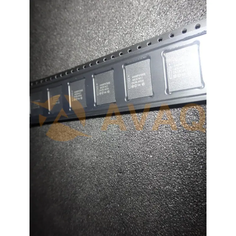
PC48F4400P0TB0EE
Datasheet:
Programmabe:
Not Verified
Memory Type:
Non-Volatile
Memory Format:
FLASH
Technology:
FLASH - NOR (MLC)
EDA/CAD Models:
Please fill in the short form below and we will provide you the quotation immediately.
Blending high density with unparalleled reliability, the PC48F4400P0TB0EE from Intel is an outstanding NAND flash memory chip. Belonging to the esteemed 3D NAND Flash product line, this chip boasts a storage capacity of 4GB and utilizes TLC technology, allowing for maximum data storage potential. As part of the 48-layer generation of Intel's 3D NAND technology, the PC48F4400P0TB0EE offers top-tier performance and is widely used in applications such as SSDs, memory cards, and other storage devices that require non-volatile, high-density storage
| Programmabe | Not Verified | Memory Type | Non-Volatile |
| Memory Format | FLASH | Technology | FLASH - NOR (MLC) |
| Memory Size | 512Mbit | Memory Organization | 32M x 16 |
| Memory Interface | CFI | Clock Frequency | 52 MHz |
| Write Cycle Time - Word, Page | - | Access Time | 95 ns |
| Voltage - Supply | 2.3V ~ 3.6V | Operating Temperature | -40°C ~ 85°C (TA) |
| Mounting Type | Surface Mount |
After-Sales & Settlement Related
 Payment
Payment Method


For alternative payment channels, please reach out to us at:
[email protected] Shipping & Packing
Shipping Method


AVAQ determines and packages all devices based on electrostatic discharge (ESD) and moisture sensitivity level (MSL) protection requirements.
 Warranty

365-Day Product
Quality Guarantee
We promise to provide 365 days quality assurance service for all our products.
| Qty. | Unit Price | Ext. Price |
|---|---|---|
| 1+ | $23.708 | $23.71 |
| 192+ | $9.460 | $1,816.32 |
| 480+ | $9.144 | $4,389.12 |
| 960+ | $8.988 | $8,628.48 |
The prices below are for reference only.
All bill of materials (BOM) can be sent via email to ![]() [email protected],
or fill below form to Quote for PC48F4400P0TB0EE, guaranteed quotes back within
[email protected],
or fill below form to Quote for PC48F4400P0TB0EE, guaranteed quotes back within
![]() 12hr.
12hr.
