Payment Method


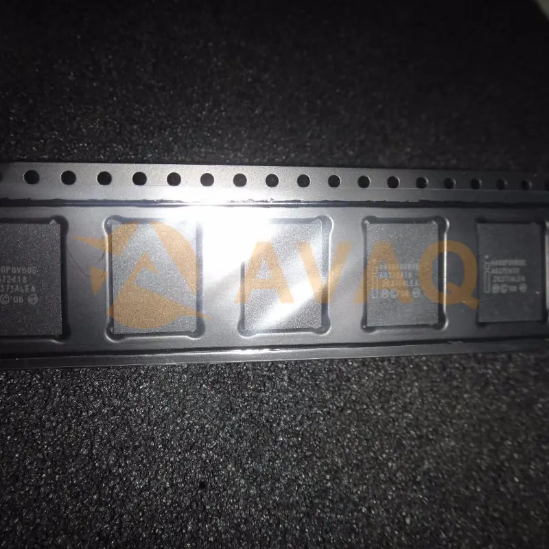
NOR Flash Parallel 512Mbit
64-EasyBGA (10x13)Manufacturer:
Micron Technology Inc.
Mfr.Part #:
PC48F4400P0VB0EE
Datasheet:
Pbfree Code:
Yes
Part Life Cycle Code:
Obsolete
Pin Count:
64
Reach Compliance Code:
compliant
EDA/CAD Models:
Please fill in the short form below and we will provide you the quotation immediately.
The PC48F4400P0VB0EE from Micron Technology is a top-of-the-line NAND flash memory chip designed for high-speed data access and reliability. With a storage capacity of 4GB and a voltage of 3.3V, this chip is ideal for use in solid-state drives (SSDs) and industrial equipment that require fast and efficient data storage. Its parallel interface and maximum clock frequency of 40MHz ensure quick and seamless data transfer, while its 2KB page size and 128KB block size allow for efficient storage and retrieval of large amounts of data. Additionally, the built-in error correction codes (ECC) and wear-leveling algorithm guarantee data integrity and prolong the lifespan of the memory cells, ensuring long-term reliability. The PC48F4400P0VB0EE is also designed to operate in a wide temperature range, making it suitable for use in a variety of environmental conditions
| Pbfree Code | Yes | Part Life Cycle Code | Obsolete |
| Pin Count | 64 | Reach Compliance Code | compliant |
| ECCN Code | EAR99 | HTS Code | 8542.32.00.51 |
| Access Time-Max | 100 ns | Additional Feature | ASYNCHRONOUS READ MODE |
| Boot Block | BOTTOM/TOP | Command User Interface | YES |
| Common Flash Interface | YES | Data Polling | NO |
| JESD-30 Code | R-PBGA-B64 | JESD-609 Code | e1 |
| Length | 13 mm | Memory Density | 536870912 bit |
| Memory IC Type | FLASH | Memory Width | 16 |
| Number of Functions | 1 | Number of Sectors/Size | 8, 510 |
| Number of Terminals | 64 | Number of Words | 33554432 words |
| Number of Words Code | 32000000 | Operating Mode | SYNCHRONOUS |
| Operating Temperature-Max | 85 °C | Operating Temperature-Min | -40 °C |
| Organization | 32MX16 | Parallel/Serial | PARALLEL |
| Peak Reflow Temperature (Cel) | 260 | Programming Voltage | 1.8 V |
| Qualification Status | Not Qualified | Seated Height-Max | 1.2 mm |
| Sector Size | 16K,64K | Standby Current-Max | 0.00042 A |
| Supply Current-Max | 0.031 mA | Supply Voltage-Max (Vsup) | 2 V |
| Supply Voltage-Min (Vsup) | 1.7 V | Supply Voltage-Nom (Vsup) | 1.8 V |
| Surface Mount | YES | Technology | CMOS |
| Temperature Grade | INDUSTRIAL | Terminal Finish | TIN SILVER COPPER |
| Terminal Form | BALL | Terminal Pitch | 1 mm |
| Terminal Position | BOTTOM | Time@Peak Reflow Temperature-Max (s) | 30 |
| Toggle Bit | NO | Type | NOR TYPE |
| Width | 10 mm |
After-Sales & Settlement Related
 Payment
Payment Method


For alternative payment channels, please reach out to us at:
[email protected] Shipping & Packing
Shipping Method


AVAQ determines and packages all devices based on electrostatic discharge (ESD) and moisture sensitivity level (MSL) protection requirements.
 Warranty

365-Day Product
Quality Guarantee
We promise to provide 365 days quality assurance service for all our products.
| Qty. | Unit Price | Ext. Price |
|---|---|---|
| 1+ | - | - |
The prices below are for reference only.
All bill of materials (BOM) can be sent via email to ![]() [email protected],
or fill below form to Quote for PC48F4400P0VB0EE, guaranteed quotes back within
[email protected],
or fill below form to Quote for PC48F4400P0VB0EE, guaranteed quotes back within
![]() 12hr.
12hr.
