Payment Method


Designed for precise timing applications in electronic devices
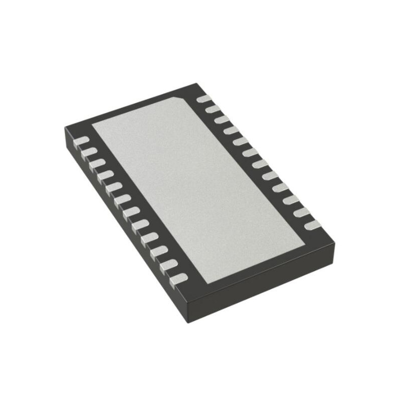
QFN-16Manufacturer:
SILICON
Mfr.Part #:
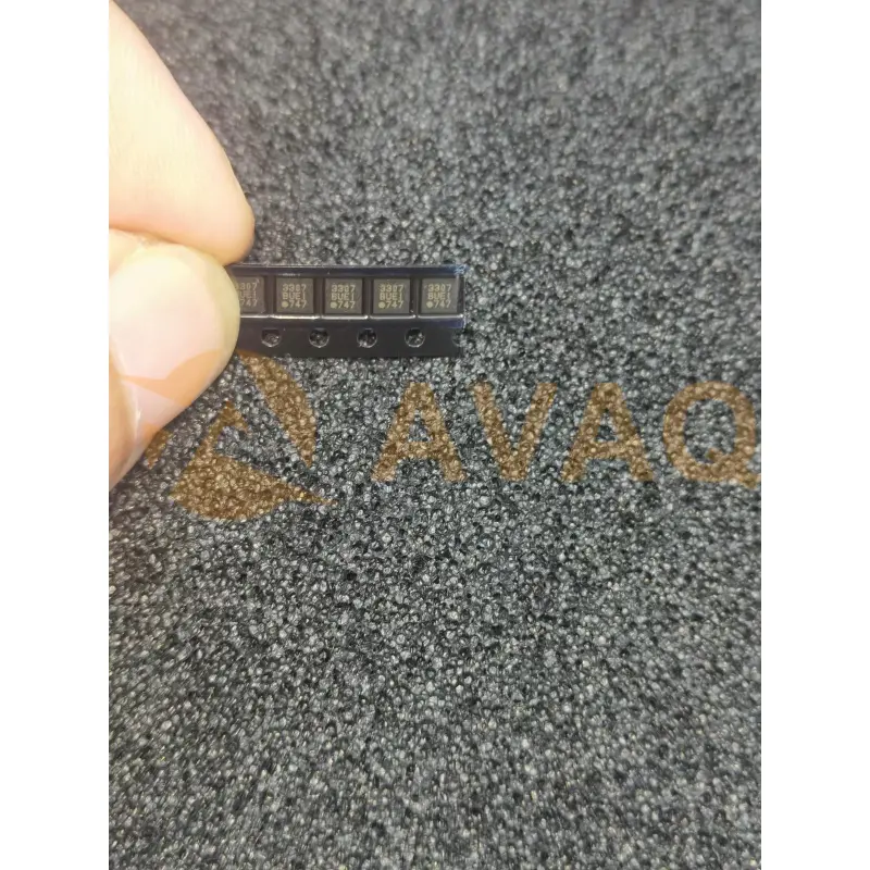
SI53307-B-GMR
Datasheet:
Part Life Cycle Code:
Active
Reach Compliance Code:
compliant
Additional Feature:
ALSO OPERATES AT 2.5 V AND 3.3 V SUPPLY
Family:
53307
EDA/CAD Models:
Please fill in the short form below and we will provide you the quotation immediately.
The SI53307-B-GMR is a versatile and highly integrated clock generator and jitter attenuator designed for various applications in telecommunications, networking, and industrial systems. With its wide range of features, including multiple clock outputs configurable up to 700 MHz, advanced jitter attenuation techniques, and support for various output formats, this device offers flexibility and high performance in system design. The integrated EEPROM makes customization and configuration of device settings effortless, while its wide supply voltage range and temperature range enhance its versatility and reliability in demanding environments. Additionally, the SI53307-B-GMR's compact package and low power consumption make it well-suited for space-constrained and power-sensitive applications
| Part Life Cycle Code | Active | Reach Compliance Code | compliant |
| Additional Feature | ALSO OPERATES AT 2.5 V AND 3.3 V SUPPLY | Family | 53307 |
| Input Conditioning | DIFFERENTIAL | JESD-30 Code | S-XQCC-N16 |
| Length | 3 mm | Logic IC Type | LOW SKEW CLOCK DRIVER |
| Number of Functions | 2 | Number of Inverted Outputs | |
| Number of Terminals | 16 | Number of True Outputs | 6 |
| Operating Temperature-Max | 85 °C | Operating Temperature-Min | -40 °C |
| Packing Method | TR | Power Supply Current-Max (ICC) | 100 mA |
| Prop. Delay@Nom-Sup | 1.075 ns | Propagation Delay (tpd) | 1.075 ns |
| Same Edge Skew-Max (tskwd) | 0.12 ns | Seated Height-Max | 0.9 mm |
| Supply Voltage-Max (Vsup) | 1.89 V | Supply Voltage-Min (Vsup) | 1.71 V |
| Supply Voltage-Nom (Vsup) | 1.8 V | Surface Mount | YES |
| Terminal Form | NO LEAD | Terminal Pitch | 0.5 mm |
| Terminal Position | QUAD | Width | 3 mm |
After-Sales & Settlement Related
 Payment
Payment Method


For alternative payment channels, please reach out to us at:
[email protected] Shipping & Packing
Shipping Method


AVAQ determines and packages all devices based on electrostatic discharge (ESD) and moisture sensitivity level (MSL) protection requirements.
 Warranty

365-Day Product
Quality Guarantee
We promise to provide 365 days quality assurance service for all our products.
| Qty. | Unit Price | Ext. Price |
|---|---|---|
| 1+ | $2.541 | $2.54 |
| 200+ | $0.985 | $197.00 |
| 500+ | $0.949 | $474.50 |
| 1000+ | $0.932 | $932.00 |
The prices below are for reference only.
All bill of materials (BOM) can be sent via email to ![]() [email protected],
or fill below form to Quote for SI53307-B-GMR, guaranteed quotes back within
[email protected],
or fill below form to Quote for SI53307-B-GMR, guaranteed quotes back within
![]() 12hr.
12hr.

AK1573
Asahi Kasei Microdevices/AKM
1000+ $2.489

MN3102
Panasonic
Durable Plastic Package for Moisture-Sensitive Environments

SI5351A-B-GT
Skyworks
Clock Generator Si5351A-B-GT PK

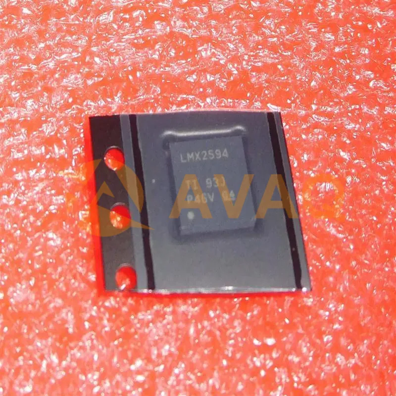
LMX2594RHAT
Texas Instruments
15-GHz wideband PLLatinum™ RF synthesizer with phase synchronization and JESD204B support 40-VQFN -40 to 85"

LM565CN
Texas Instruments
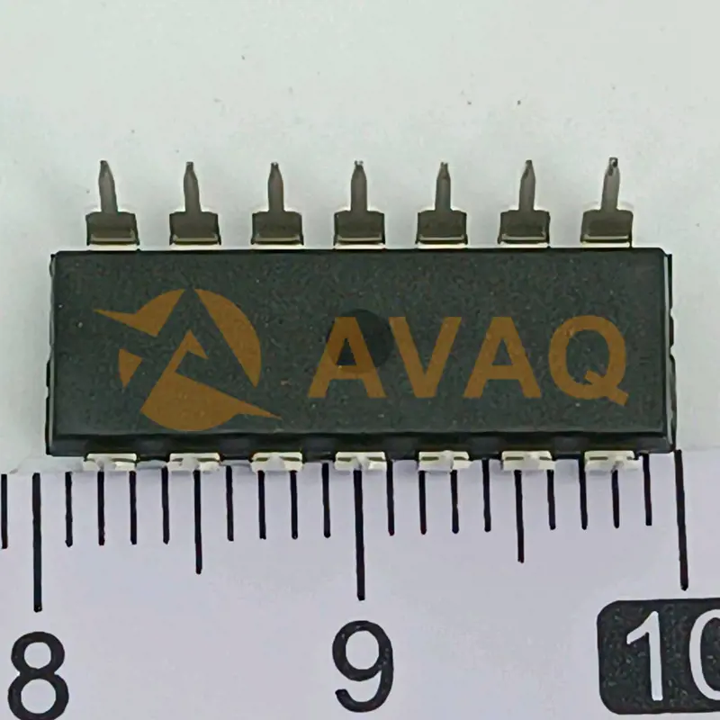
PLL Single 0.25MHz to 0.5MHz 14-Pin MDIP Rail
