Payment Method


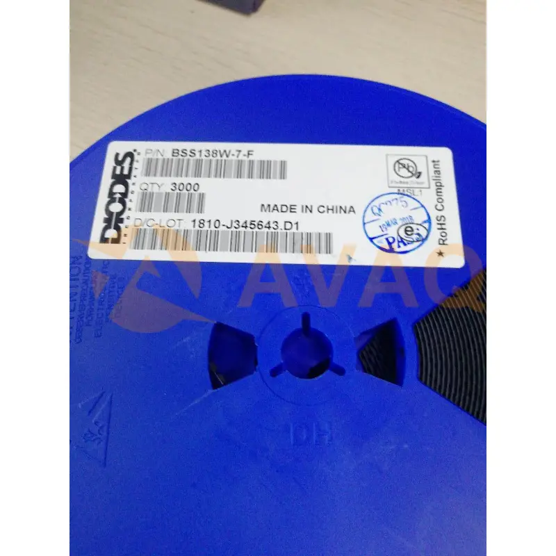
BSS138W-7-F is an N-channel MOSFET with a SOT323 package, designed to operate at voltages up to 50V and currents up to 0.2A
SOT-323-3Manufacturer:
Mfr.Part #:
BSS138W-7-F
Datasheet:
Pbfree Code:
Yes
Part Life Cycle Code:
Active
Pin Count:
3
Reach Compliance Code:
compliant
EDA/CAD Models:
Send all BOMs to ![]() [email protected],
or fill out the form below for a quote on BSS138W-7-F. Guaranteed response within
[email protected],
or fill out the form below for a quote on BSS138W-7-F. Guaranteed response within
![]() 12hr.
12hr.
Please fill in the short form below and we will provide you the quotation immediately.
The BSS138W-7-F is a small signal N-channel MOSFET transistor that is well-suited for general-purpose switching applications in digital circuits. With a maximum drain-source voltage rating of 50V and a continuous drain current of 220mA, this transistor delivers reliable performance in various electronic systems. Its low on-resistance of 3.5 ohms makes it ideal for low voltage and low power applications, ensuring efficient operation. Housed in a compact SOT-323 package, the BSS138W-7-F offers space-saving advantages for designs with limited space, while its gate-source voltage of ±8V and threshold voltage of 1 to 2V provide compatibility with a diverse range of circuitry. With its fast switching speed, this transistor is suitable for applications requiring quick response times, making it a valuable component for digital circuit design
| Pbfree Code | Yes | Part Life Cycle Code | Active |
| Pin Count | 3 | Reach Compliance Code | compliant |
| ECCN Code | EAR99 | HTS Code | 8541.21.00.95 |
| Factory Lead Time | 63 Weeks | Additional Feature | LOW THRESHOLD |
| Configuration | SINGLE WITH BUILT-IN DIODE | DS Breakdown Voltage-Min | 50 V |
| Drain Current-Max (ID) | 0.2 A | Drain-source On Resistance-Max | 3.5 Ω |
| FET Technology | METAL-OXIDE SEMICONDUCTOR | Feedback Cap-Max (Crss) | 8 pF |
| JESD-30 Code | R-PDSO-G3 | JESD-609 Code | e3 |
| Moisture Sensitivity Level | 1 | Number of Elements | 1 |
| Number of Terminals | 3 | Operating Mode | ENHANCEMENT MODE |
| Operating Temperature-Max | 150 °C | Operating Temperature-Min | -55 °C |
| Peak Reflow Temperature (Cel) | 260 | Polarity/Channel Type | N-CHANNEL |
| Power Dissipation Ambient-Max | 0.2 W | Power Dissipation-Max (Abs) | 0.2 W |
| Qualification Status | Not Qualified | Reference Standard | UL RECOGNIZED |
| Surface Mount | YES | Terminal Finish | MATTE TIN |
| Terminal Form | GULL WING | Terminal Position | DUAL |
| Time@Peak Reflow Temperature-Max (s) | 30 | Transistor Application | SWITCHING |
| Transistor Element Material | SILICON |
After-Sales & Settlement Related
 Payment
Payment Method


For alternative payment channels, please reach out to us at:
[email protected] Shipping & Packing
Shipping Method


AVAQ determines and packages all devices based on electrostatic discharge (ESD) and moisture sensitivity level (MSL) protection requirements.
 Warranty

365-Day Product
Quality Guarantee
We promise to provide 365 days quality assurance service for all our products.
| Qty. | Unit Price | Ext. Price |
|---|---|---|
| 10+ | $0.030 | $0.30 |
| 100+ | $0.026 | $2.60 |
| 300+ | $0.024 | $7.20 |
| 3000+ | $0.023 | $69.00 |
| 6000+ | $0.021 | $126.00 |
| 9000+ | $0.021 | $189.00 |
The prices below are for reference only.
