Payment Method


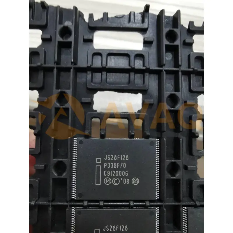
High-speed Numonyx Flash
TSOP-56Manufacturer:
Alliance Memory, Inc.
Mfr.Part #:
JS28F128P33BF70A
Datasheet:
Programmabe:
Not Verified
Memory Type:
Non-Volatile
Memory Format:
FLASH
Technology:
FLASH - NOR
EDA/CAD Models:
Please fill in the short form below and we will provide you the quotation immediately.
Organized into 64 sectors of 128KB each, the JS28F128P33BF70A also includes eight 1KB boot blocks for added flexibility and functionality. Its parallel interface simplifies integration into embedded systems, allowing for seamless operation within a range of devices. Additionally, this Flash memory chip boasts exceptional reliability and endurance, guaranteeing a minimum of 100,000 program/erase cycles per sector
| Programmabe | Not Verified | Memory Type | Non-Volatile |
| Memory Format | FLASH | Technology | FLASH - NOR |
| Memory Size | 128Mbit | Memory Organization | 8M x 16 |
| Memory Interface | Parallel | Clock Frequency | 52 MHz |
| Write Cycle Time - Word, Page | 70ns | Access Time | 70 ns |
| Voltage - Supply | 2.3V ~ 3.6V | Operating Temperature | -40°C ~ 85°C (TC) |
| Mounting Type | Surface Mount |
After-Sales & Settlement Related
 Payment
Payment Method


For alternative payment channels, please reach out to us at:
[email protected] Shipping & Packing
Shipping Method


AVAQ determines and packages all devices based on electrostatic discharge (ESD) and moisture sensitivity level (MSL) protection requirements.
 Warranty

365-Day Product
Quality Guarantee
We promise to provide 365 days quality assurance service for all our products.
| Qty. | Unit Price | Ext. Price |
|---|---|---|
| 1+ | $14.769 | $14.77 |
| 192+ | $5.893 | $1,131.46 |
| 480+ | $5.696 | $2,734.08 |
| 960+ | $5.601 | $5,376.96 |
The prices below are for reference only.
All bill of materials (BOM) can be sent via email to ![]() [email protected],
or fill below form to Quote for JS28F128P33BF70A, guaranteed quotes back within
[email protected],
or fill below form to Quote for JS28F128P33BF70A, guaranteed quotes back within
![]() 12hr.
12hr.
