Payment Method


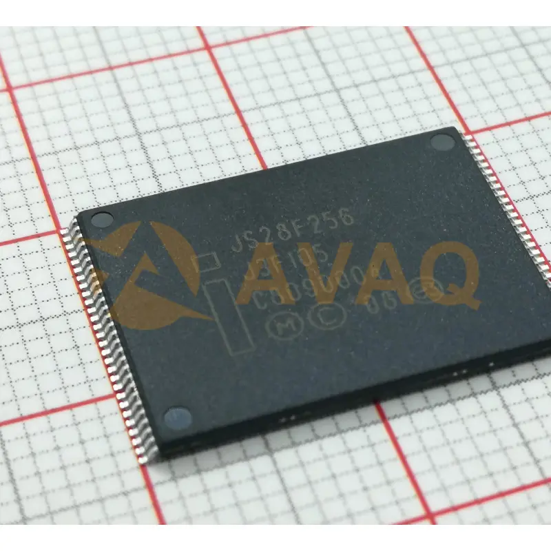
32M x 8bit memory
TSOP-56Manufacturer:
Micron Technology Inc.
Mfr.Part #:
JS28F256J3F105A
Datasheet:
Pbfree Code:
Yes
Part Life Cycle Code:
Obsolete
Pin Count:
56
Reach Compliance Code:
compliant
EDA/CAD Models:
Please fill in the short form below and we will provide you the quotation immediately.
In addition to its impressive performance capabilities, the JS28F256J3F105A chip also prioritizes data protection. It features a hardware data protection mechanism and offers various software protection options, ensuring that your valuable data remains secure. Furthermore, this flash memory chip utilizes a 16-bit data interface, further enhancing its compatibility and usability in a wide range of devices and applications. Its compliance with RoHS standards also demonstrates Intel's commitment to environmental sustainability
| Pbfree Code | Yes | Part Life Cycle Code | Obsolete |
| Pin Count | 56 | Reach Compliance Code | compliant |
| ECCN Code | EAR99 | HTS Code | 8542.32.00.51 |
| Access Time-Max | 105 ns | Alternate Memory Width | 8 |
| JESD-30 Code | R-PDSO-G56 | JESD-609 Code | e3 |
| Length | 18.4 mm | Memory Density | 268435456 bit |
| Memory IC Type | FLASH | Memory Width | 16 |
| Moisture Sensitivity Level | 3 | Number of Functions | 1 |
| Number of Terminals | 56 | Number of Words | 16777216 words |
| Number of Words Code | 16000000 | Operating Mode | ASYNCHRONOUS |
| Operating Temperature-Max | 85 °C | Operating Temperature-Min | -40 °C |
| Organization | 16MX16 | Parallel/Serial | PARALLEL |
| Peak Reflow Temperature (Cel) | 260 | Programming Voltage | 2.7 V |
| Qualification Status | Not Qualified | Seated Height-Max | 1.2 mm |
| Supply Voltage-Max (Vsup) | 3.6 V | Supply Voltage-Min (Vsup) | 2.7 V |
| Supply Voltage-Nom (Vsup) | 3 V | Surface Mount | YES |
| Technology | CMOS | Temperature Grade | INDUSTRIAL |
| Terminal Finish | Matte Tin (Sn) | Terminal Form | GULL WING |
| Terminal Pitch | 0.5 mm | Terminal Position | DUAL |
| Time@Peak Reflow Temperature-Max (s) | 30 | Type | NOR TYPE |
| Width | 14 mm |
After-Sales & Settlement Related
 Payment
Payment Method


For alternative payment channels, please reach out to us at:
[email protected] Shipping & Packing
Shipping Method


AVAQ determines and packages all devices based on electrostatic discharge (ESD) and moisture sensitivity level (MSL) protection requirements.
 Warranty

365-Day Product
Quality Guarantee
We promise to provide 365 days quality assurance service for all our products.
| Qty. | Unit Price | Ext. Price |
|---|---|---|
| 1+ | - | - |
The prices below are for reference only.
All bill of materials (BOM) can be sent via email to ![]() [email protected],
or fill below form to Quote for JS28F256J3F105A, guaranteed quotes back within
[email protected],
or fill below form to Quote for JS28F256J3F105A, guaranteed quotes back within
![]() 12hr.
12hr.
