Payment Method


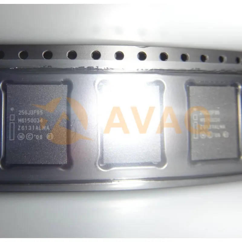
This NOR flash memory chip is supplied in a tray format for easy handling and storage during manufacturing processes
BGA-64Manufacturer:
Micron Technology Inc.
Mfr.Part #:
PC28F256J3F95A
Datasheet:
Programmabe:
Not Verified
Memory Type:
Non-Volatile
Memory Format:
FLASH
Technology:
FLASH - NOR
EDA/CAD Models:
Send all BOMs to ![]() [email protected],
or fill out the form below for a quote on PC28F256J3F95A. Guaranteed response within
[email protected],
or fill out the form below for a quote on PC28F256J3F95A. Guaranteed response within
![]() 12hr.
12hr.
Please fill in the short form below and we will provide you the quotation immediately.
The PC28F256J3F95A from Micron Technology is a versatile NAND Flash memory chip that offers impressive storage capacity and high-speed data access. Designed for compatibility with a range of embedded systems, including automotive, industrial, and consumer electronics, this chip is well-suited for a variety of applications requiring reliable performance and efficient data storage. Its compact 48-ball fine pitch ball grid array (FBGA) package type makes it easy to integrate into existing designs, while its extended voltage range of 2.7V to 3.6V ensures flexibility in powering options. This NAND Flash memory chip is known for its fast read and program times, making it ideal for tasks such as firmware storage, boot code storage, and data logging. Its durable construction allows for use in harsh environmental conditions, providing a dependable solution for demanding applications
| Programmabe | Not Verified | Memory Type | Non-Volatile |
| Memory Format | FLASH | Technology | FLASH - NOR |
| Memory Size | 256Mbit | Memory Organization | 32M x 8, 16M x 16 |
| Memory Interface | Parallel | Clock Frequency | - |
| Write Cycle Time - Word, Page | 95ns | Access Time | 95 ns |
| Voltage - Supply | 2.7V ~ 3.6V | Operating Temperature | -40°C ~ 85°C (TA) |
| Mounting Type | Surface Mount |
After-Sales & Settlement Related
 Payment
Payment Method


For alternative payment channels, please reach out to us at:
[email protected] Shipping & Packing
Shipping Method


AVAQ determines and packages all devices based on electrostatic discharge (ESD) and moisture sensitivity level (MSL) protection requirements.
 Warranty

365-Day Product
Quality Guarantee
We promise to provide 365 days quality assurance service for all our products.
| Qty. | Unit Price | Ext. Price |
|---|---|---|
| 1+ | $28.256 | $28.26 |
| 200+ | $11.275 | $2,255.00 |
| 500+ | $10.898 | $5,449.00 |
| 864+ | $10.712 | $9,255.17 |
The prices below are for reference only.
