Payment Method


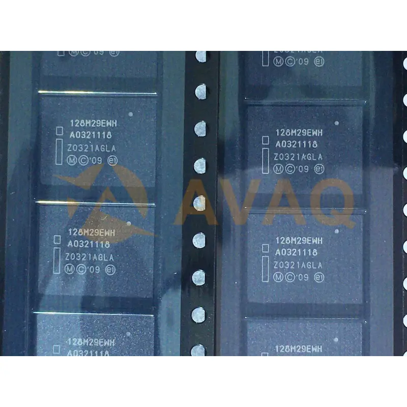
Details on the PC28F128M29EWHF product, which is a NOR Flash memory chip with 8MX16 configuration and SLC technology
BGA-64Manufacturer:
Micron Technology Inc.
Mfr.Part #:
PC28F128M29EWHF
Datasheet:
Programmabe:
Not Verified
Memory Type:
Non-Volatile
Memory Format:
FLASH
Technology:
FLASH - NOR
EDA/CAD Models:
Send all BOMs to ![]() [email protected],
or fill out the form below for a quote on PC28F128M29EWHF. Guaranteed response within
[email protected],
or fill out the form below for a quote on PC28F128M29EWHF. Guaranteed response within
![]() 12hr.
12hr.
Please fill in the short form below and we will provide you the quotation immediately.
In addition to its exceptional speed and versatility, the PC28F128M29EWHF is designed with advanced features to ensure data integrity and longevity. It incorporates hardware and software protection mechanisms to prevent data corruption, providing peace of mind for users. Furthermore, its high endurance of up to 100,000 program/erase cycles reinforces its durability, making it a reliable choice for demanding applications that require consistent performance over an extended period
| Programmabe | Not Verified | Memory Type | Non-Volatile |
| Memory Format | FLASH | Technology | FLASH - NOR |
| Memory Size | 128Mbit | Memory Organization | 16M x 8, 8M x 16 |
| Memory Interface | Parallel | Clock Frequency | - |
| Write Cycle Time - Word, Page | 60ns | Access Time | 60 ns |
| Voltage - Supply | 2.7V ~ 3.6V | Operating Temperature | -40°C ~ 85°C (TA) |
| Mounting Type | Surface Mount |
After-Sales & Settlement Related
 Payment
Payment Method


For alternative payment channels, please reach out to us at:
[email protected] Shipping & Packing
Shipping Method


AVAQ determines and packages all devices based on electrostatic discharge (ESD) and moisture sensitivity level (MSL) protection requirements.
 Warranty

365-Day Product
Quality Guarantee
We promise to provide 365 days quality assurance service for all our products.
| Qty. | Unit Price | Ext. Price |
|---|---|---|
| 1+ | $6.959 | $6.96 |
| 200+ | $2.776 | $555.20 |
| 500+ | $2.684 | $1,342.00 |
| 1104+ | $2.639 | $2,913.46 |
The prices below are for reference only.
