Payment Method


Energy-efficient with only 31mA current consumption
BGA-64Manufacturer:
Micron Technology Inc.
Mfr.Part #:
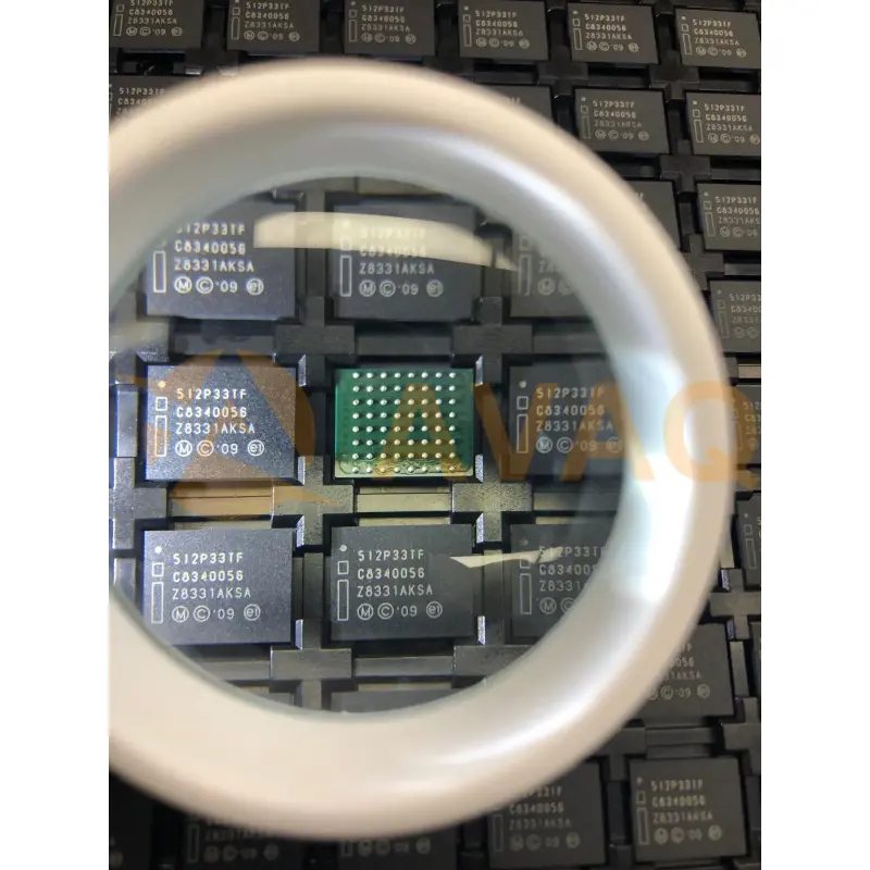
PC28F512P33TFA
Datasheet:
Programmabe:
Not Verified
Memory Type:
Non-Volatile
Memory Format:
FLASH
Technology:
FLASH - NOR
EDA/CAD Models:
Send all BOMs to ![]() [email protected],
or fill out the form below for a quote on PC28F512P33TFA. Guaranteed response within
[email protected],
or fill out the form below for a quote on PC28F512P33TFA. Guaranteed response within
![]() 12hr.
12hr.
Please fill in the short form below and we will provide you the quotation immediately.
Designed for durability and reliability, the PC28F512P33TFA guarantees a minimum of 100,000 program/erase cycles, demonstrating its robust quality and long lifespan. In addition to its high capacity and fast speeds, this NAND Flash memory device offers advanced protection features, including hardware data protection and software-based security measures. These additional layers of security ensure that sensitive information stored on the device remains safe and secure at all times, making it a reliable choice for data storage in various embedded systems
| Programmabe | Not Verified | Memory Type | Non-Volatile |
| Memory Format | FLASH | Technology | FLASH - NOR |
| Memory Size | 512Mbit | Memory Organization | 32M x 16 |
| Memory Interface | Parallel | Clock Frequency | 52 MHz |
| Write Cycle Time - Word, Page | 95ns | Access Time | 95 ns |
| Voltage - Supply | 2.3V ~ 3.6V | Operating Temperature | -40°C ~ 85°C (TA) |
| Mounting Type | Surface Mount |
After-Sales & Settlement Related
 Payment
Payment Method


For alternative payment channels, please reach out to us at:
[email protected] Shipping & Packing
Shipping Method


AVAQ determines and packages all devices based on electrostatic discharge (ESD) and moisture sensitivity level (MSL) protection requirements.
 Warranty

365-Day Product
Quality Guarantee
We promise to provide 365 days quality assurance service for all our products.
| Qty. | Unit Price | Ext. Price |
|---|---|---|
| 1+ | $25.915 | $25.92 |
| 200+ | $10.341 | $2,068.20 |
| 500+ | $9.995 | $4,997.50 |
| 1000+ | $9.825 | $9,825.00 |
The prices below are for reference only.
