Payment Method


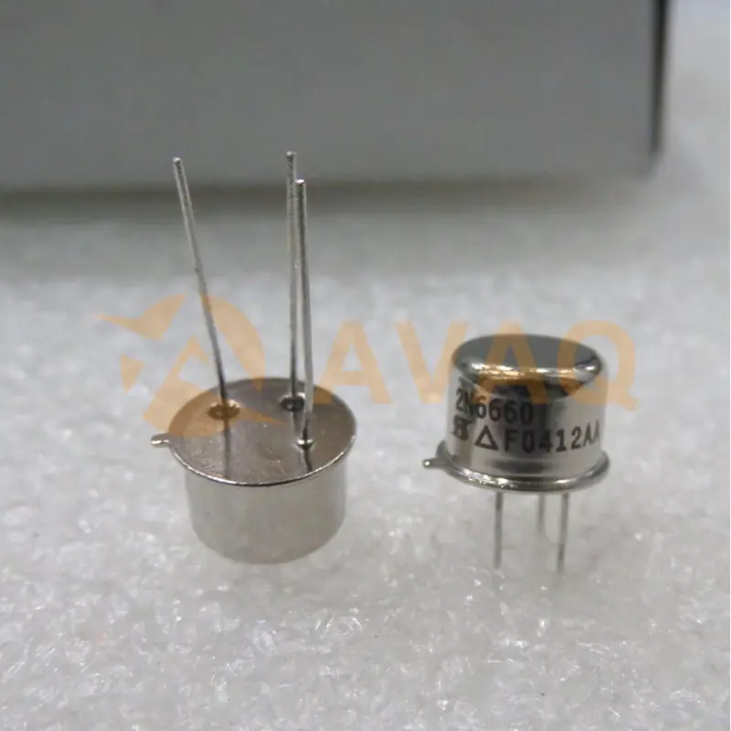
60V, 3 Ohm, N-Channel, Enhancement-Mode, Vertical DMOS FET.
TO-205AD (TO-39)Manufacturer:
Solid State Inc.
Mfr.Part #:
2N6660
Datasheet:
Part Life Cycle Code:
Active
Reach Compliance Code:
compliant
ECCN Code:
EAR99
HTS Code:
8542.39.00.01
EDA/CAD Models:
All bill of materials (BOM) can be sent via email to ![]() [email protected],
or fill below form to Quote for 2N6660, guaranteed quotes back within
[email protected],
or fill below form to Quote for 2N6660, guaranteed quotes back within
![]() 12hr.
12hr.
Please fill in the short form below and we will provide you the quotation immediately.
The 2N6660 is a cutting-edge enhancement-mode transistor that capitalizes on vertical DMOS technology and a time-tested silicon-gate manufacturing process. This winning combination results in a device that boasts the power handling capabilities of bipolar transistors, along with the high input impedance and positive temperature coefficient characteristic of MOS devices. Thanks to its MOS structure, the 2N6660 is immune to thermal runaway and thermally-induced secondary breakdown. This makes it an excellent choice for a wide range of switching and amplifying applications, where low threshold voltage, high breakdown voltage, high input impedance, low input capacitance, and fast switching speeds are crucial. Whether you need a reliable component for your next electronics project or a dependable solution for industrial applications, the 2N6660 is up to the task
| Source Content uid | 2N6660 | Part Life Cycle Code | Active |
| Reach Compliance Code | compliant | ECCN Code | EAR99 |
| HTS Code | 8542.39.00.01 | Factory Lead Time | 4 Weeks |
| Additional Feature | HIGH INPUT IMPEDANCE | Case Connection | DRAIN |
| Configuration | SINGLE WITH BUILT-IN DIODE | DS Breakdown Voltage-Min | 60 V |
| Drain Current-Max (ID) | 0.41 A | Drain-source On Resistance-Max | 3 Ω |
| FET Technology | METAL-OXIDE SEMICONDUCTOR | Feedback Cap-Max (Crss) | 10 pF |
| JEDEC-95 Code | TO-39 | JESD-30 Code | O-MBCY-W3 |
| JESD-609 Code | e4 | Number of Elements | 1 |
| Number of Terminals | 3 | Operating Mode | ENHANCEMENT MODE |
| Operating Temperature-Max | 150 °C | Operating Temperature-Min | -55 °C |
| Polarity/Channel Type | N-CHANNEL | Power Dissipation Ambient-Max | 6.25 W |
| Power Dissipation-Max (Abs) | 6.25 W | Pulsed Drain Current-Max (IDM) | 3 A |
| Qualification Status | Not Qualified | Reference Standard | TS 16949 |
| Surface Mount | NO | Terminal Finish | NICKEL GOLD |
| Terminal Form | WIRE | Terminal Position | BOTTOM |
| Transistor Application | SWITCHING | Transistor Element Material | SILICON |
| Turn-off Time-Max (toff) | 10 ns | Turn-on Time-Max (ton) | 10 ns |
After-Sales & Settlement Related
 Payment
Payment Method


For alternative payment channels, please reach out to us at:
[email protected] Shipping & Packing
Shipping Method


AVAQ determines and packages all devices based on electrostatic discharge (ESD) and moisture sensitivity level (MSL) protection requirements.
 Warranty

365-Day Product
Quality Guarantee
We promise to provide 365 days quality assurance service for all our products.
| Qty. | Unit Price | Ext. Price |
|---|---|---|
| 1+ | $22.703 | $22.70 |
| 30+ | $21.782 | $653.46 |
The prices below are for reference only.
2N2222
Stmicroelectronics
1000+ $0.587
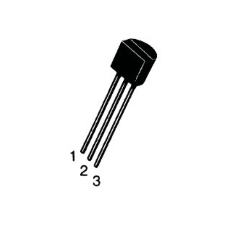
BC547
Onsemi
NPN Epitaxial Silicon Transistor
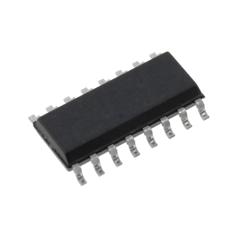
ULN2003
Onsemi
Versatile device for driving heavy loads and motor
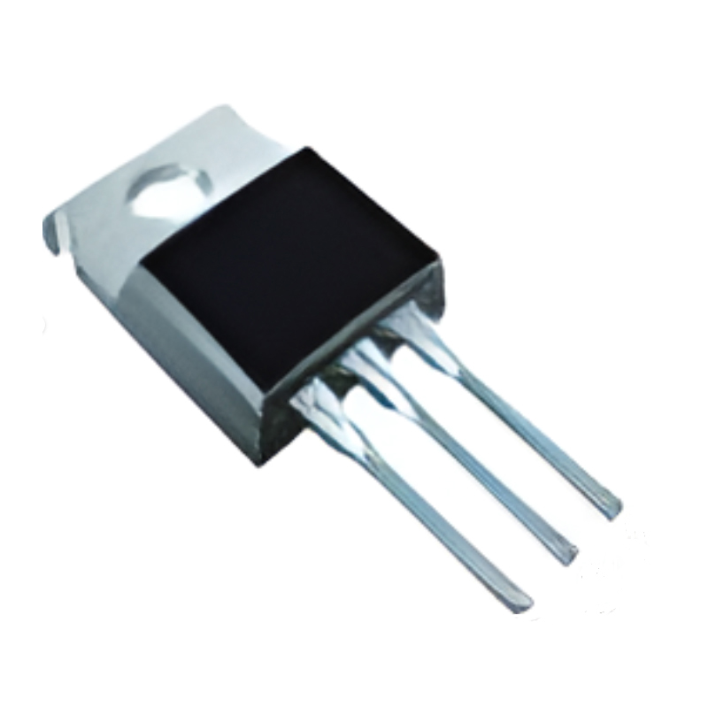
IRF3205
Infineon
TO-220AB Tube Power Transistor with N-Channel Silicon

TAN15
Microchip
The TAN is a robust NPN transistor designed for high-frequency applications, capable of operating at up to V and continuous curren
