Payment Method


Asymmetric Dual N-Channel PowerTrench® Power Stage MOSFET 30V
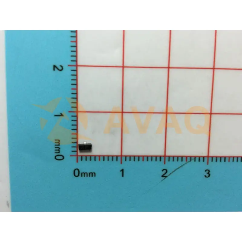
PQFN-8Manufacturer:
onsemi
Mfr.Part #:
FDMS3668S
Datasheet:
Technology:
Si
Mounting Style:
SMD/SMT
Transistor Polarity:
N-Channel
Number Of Channels:
2 Channel
EDA/CAD Models:
All bill of materials (BOM) can be sent via email to ![]() [email protected],
or fill below form to Quote for FDMS3668S, guaranteed quotes back within
[email protected],
or fill below form to Quote for FDMS3668S, guaranteed quotes back within
![]() 12hr.
12hr.
Please fill in the short form below and we will provide you the quotation immediately.
The FDMS3668S is a specialized device featuring two N-Channel MOSFETs in a dual PQFN package. Its switch node has been internally connected to allow for convenient placement and routing of synchronous buck converters. The control MOSFET (Q1) and synchronousSyncFET (Q2) are specifically designed to deliver optimal power efficiency, making this device an ideal choice for applications requiring high performance and reliable power management
| Product Category | MOSFET | Technology | Si |
| Mounting Style | SMD/SMT | Transistor Polarity | N-Channel |
| Number of Channels | 2 Channel | Vds - Drain-Source Breakdown Voltage | 30 V |
| Id - Continuous Drain Current | 13 A, 18 A | Rds On - Drain-Source Resistance | 8 mOhms, 5 mOhms |
| Vgs - Gate-Source Voltage | - 20 V, + 20 V, - 12 V, + 12 V | Vgs th - Gate-Source Threshold Voltage | 1.1 V |
| Qg - Gate Charge | 29 nC, 38 nC | Minimum Operating Temperature | - 55 C |
| Maximum Operating Temperature | + 150 C | Pd - Power Dissipation | 2.2 W, 2.5 W |
| Channel Mode | Enhancement | Tradename | Power Stage PowerTrench |
| Series | FDMS3668S | Configuration | Dual |
| Height | 1.1 mm | Length | 6 mm |
| Product Type | MOSFET | Factory Pack Quantity | 3000 |
| Subcategory | MOSFETs | Transistor Type | 2 N-Channel |
| Width | 5 mm | Unit Weight | 0.006032 oz |
| Source Content uid | FDMS3668S | Pbfree Code | Yes |
| Part Life Cycle Code | End Of Life | Reach Compliance Code | not_compliant |
| ECCN Code | EAR99 | Factory Lead Time | 4 Weeks |
| Case Connection | DRAIN SOURCE | DS Breakdown Voltage-Min | 30 V |
| Drain Current-Max (Abs) (ID) | 60 A | Drain Current-Max (ID) | 13 A |
| Drain-source On Resistance-Max | 0.008 Ω | FET Technology | METAL-OXIDE SEMICONDUCTOR |
| Feedback Cap-Max (Crss) | 70 pF | JEDEC-95 Code | MO-240AA |
| JESD-30 Code | R-PDSO-F6 | JESD-609 Code | e3 |
| Moisture Sensitivity Level | 1 | Number of Elements | 2 |
| Number of Terminals | 6 | Operating Mode | ENHANCEMENT MODE |
| Operating Temperature-Max | 150 °C | Peak Reflow Temperature (Cel) | 260 |
| Polarity/Channel Type | N-CHANNEL | Power Dissipation-Max (Abs) | 2.5 W |
| Surface Mount | YES | Terminal Finish | Tin (Sn) |
| Terminal Form | FLAT | Terminal Position | DUAL |
| Time@Peak Reflow Temperature-Max (s) | 30 | Transistor Application | SWITCHING |
| Transistor Element Material | SILICON |
After-Sales & Settlement Related
 Payment
Payment Method


For alternative payment channels, please reach out to us at:
[email protected] Shipping & Packing
Shipping Method


AVAQ determines and packages all devices based on electrostatic discharge (ESD) and moisture sensitivity level (MSL) protection requirements.
 Warranty

365-Day Product
Quality Guarantee
We promise to provide 365 days quality assurance service for all our products.
| Qty. | Unit Price | Ext. Price |
|---|---|---|
| 1+ | $1.866 | $1.87 |
| 200+ | $0.722 | $144.40 |
| 500+ | $0.698 | $349.00 |
| 1000+ | $0.685 | $685.00 |
The prices below are for reference only.

2N2222
Stmicroelectronics
1000+ $0.587

BC547
Onsemi
NPN Epitaxial Silicon Transistor

ULN2003
Onsemi
Versatile device for driving heavy loads and motor

IRF3205
Infineon
TO-220AB Tube Power Transistor with N-Channel Silicon

TAN15
Microchip
The TAN is a robust NPN transistor designed for high-frequency applications, capable of operating at up to V and continuous curren