Payment Method


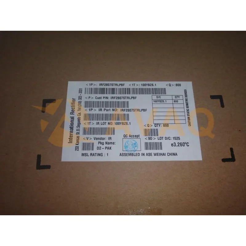
Plastic D2PAK-3 package for easy installation and handling
D2PAKManufacturer:
Mfr.Part #:
IRF2807S
Datasheet:
Part Life Cycle Code:
Active
Reach Compliance Code:
not_compliant
ECCN Code:
EAR99
HTS Code:
8541.29.00.95
EDA/CAD Models:
Send all BOMs to ![]() [email protected],
or fill out the form below for a quote on IRF2807S. Guaranteed response within
[email protected],
or fill out the form below for a quote on IRF2807S. Guaranteed response within
![]() 12hr.
12hr.
Please fill in the short form below and we will provide you the quotation immediately.
Step into the realm of high-efficiency power switching with the IRF2807S power MOSFET. Engineered to handle drain-to-source voltages of up to 75 volts and continuous drain currents of 82 amperes, this N-channel device is your go-to solution for power conversion and motor control applications. Its impressively low on-resistance of 8 milliohms paves the way for minimized power wastage and superior efficiency in high-power circuits. Furthermore, the IRF2807S showcases a modest 73nC gate charge, guaranteeing swift switching speeds and flawless high-frequency operation. Packaged in a TO-263 enclosure, this MOSFET promises outstanding thermal conductivity and rugged reliability, ensuring peak performance even in the most demanding conditions. Plus, its RoHS compliance underscores its eco-friendly design, making it a versatile and sustainable choice for a wide range of applications
| Part Life Cycle Code | Active | Reach Compliance Code | not_compliant |
| ECCN Code | EAR99 | HTS Code | 8541.29.00.95 |
| Additional Feature | AVALANCHE RATED, HIGH RELIABILITY, ULTRA LOW RESISTANCE | Avalanche Energy Rating (Eas) | 340 mJ |
| Case Connection | DRAIN | Configuration | SINGLE WITH BUILT-IN DIODE |
| DS Breakdown Voltage-Min | 75 V | Drain Current-Max (ID) | 75 A |
| Drain-source On Resistance-Max | 0.013 Ω | FET Technology | METAL-OXIDE SEMICONDUCTOR |
| JESD-30 Code | R-PSSO-G2 | JESD-609 Code | e0 |
| Moisture Sensitivity Level | 1 | Number of Elements | 1 |
| Number of Terminals | 2 | Operating Mode | ENHANCEMENT MODE |
| Operating Temperature-Max | 175 °C | Peak Reflow Temperature (Cel) | 225 |
| Polarity/Channel Type | N-CHANNEL | Power Dissipation Ambient-Max | 150 W |
| Pulsed Drain Current-Max (IDM) | 280 A | Qualification Status | Not Qualified |
| Surface Mount | YES | Terminal Finish | TIN LEAD |
| Terminal Form | GULL WING | Terminal Position | SINGLE |
| Time@Peak Reflow Temperature-Max (s) | 30 | Transistor Application | SWITCHING |
| Transistor Element Material | SILICON |
After-Sales & Settlement Related
 Payment
Payment Method


For alternative payment channels, please reach out to us at:
[email protected] Shipping & Packing
Shipping Method


AVAQ determines and packages all devices based on electrostatic discharge (ESD) and moisture sensitivity level (MSL) protection requirements.
 Warranty

365-Day Product
Quality Guarantee
We promise to provide 365 days quality assurance service for all our products.
| Qty. | Unit Price | Ext. Price |
|---|---|---|
| 1+ | - | - |
The prices below are for reference only.
