Payment Method


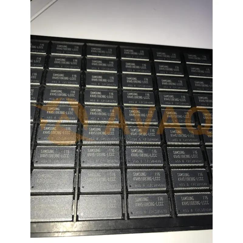
DDR DRAM, 64MX8, 0.65ns, CMOS, PDSO66,
TSOPManufacturer:
Mfr.Part #:
K4H510838G-LCCC
Datasheet:
ECCN (US):
EAR99
HTS:
8541.29.00.95
SVHC:
Yes
SVHC Exceeds Threshold:
Yes
EDA/CAD Models:
Send all BOMs to ![]() [email protected],
or fill out the form below for a quote on K4H510838G-LCCC. Guaranteed response within
[email protected],
or fill out the form below for a quote on K4H510838G-LCCC. Guaranteed response within
![]() 12hr.
12hr.
Please fill in the short form below and we will provide you the quotation immediately.
VDD : 2.5V0.2V, VDDQ : 2.5V0.2V for DDR266, 333
VDD : 2.6V0.1V, VDDQ : 2.6V0.1V for DDR400
Double-data-rate architecture; two data transfers per clock cycle
Bidirectional data strobe [DQS] (x4,x8) & [L(U)DQS] (x16)
Four banks operation
Differential clock inputs(CK and CK)
DLL aligns DQ and DQS transition with CK transition
MRS cycle with address key programs
-. Read latency : DDR266(2.5 Clock), DDR333(2.5 Clock), DDR400(3 Clock)
-. Burst length (2, 4, 8)
-. Burst type (sequential & interleave)
All inputs except data & DM are sampled at the positive going edge of the system clock(CK)
Data I/O transactions on both edges of data strobe
Edge aligned data output, center aligned data input
LDM,UDM for write masking only (x16)
DM for write masking only (x4, x8)
Auto & Self refresh
7.8us refresh interval(8K/64ms refresh)
Maximum burst refresh cycle : 8
66pin TSOP II Lead-Free & Halogen-Free package
RoHS compliant
| ECCN (US) | EAR99 | Part Status | Active |
| HTS | 8541.29.00.95 | SVHC | Yes |
| SVHC Exceeds Threshold | Yes | Automotive | No |
| PPAP | No | Category | Power MOSFET |
| Configuration | Single | Process Technology | TrenchFET |
| Channel Mode | Enhancement | Channel Type | P |
| Number of Elements per Chip | 1 | Maximum Drain Source Voltage (V) | 40 |
| Maximum Gate Source Voltage (V) | ±20 | Maximum Gate Threshold Voltage (V) | 4 |
| Operating Junction Temperature (°C) | -55 to 175 | Maximum Continuous Drain Current (A) | 110 |
| Maximum Gate Source Leakage Current (nA) | 100 | Maximum IDSS (uA) | 1 |
| Maximum Drain Source Resistance (mOhm) | 5@10V | Typical Gate Charge @ Vgs (nC) | 185@10V |
| Typical Gate Charge @ 10V (nC) | 185 | Typical Gate to Drain Charge (nC) | 42 |
| Typical Gate to Source Charge (nC) | 48 | Typical Reverse Recovery Charge (nC) | 130 |
| Typical Input Capacitance @ Vds (pF) | 11300@25V | Typical Reverse Transfer Capacitance @ Vds (pF) | 1000@25V |
| Minimum Gate Threshold Voltage (V) | 2 | Typical Output Capacitance (pF) | 1510 |
| Maximum Power Dissipation (mW) | 15000 | Typical Fall Time (ns) | 35 |
| Typical Rise Time (ns) | 290 | Typical Turn-Off Delay Time (ns) | 110 |
| Typical Turn-On Delay Time (ns) | 25 | Minimum Operating Temperature (°C) | -55 |
| Maximum Operating Temperature (°C) | 175 | Packaging | Tape and Reel |
| Maximum Power Dissipation on PCB @ TC=25°C (W) | 15 | Maximum Pulsed Drain Current @ TC=25°C (A) | 240 |
| Maximum Junction Ambient Thermal Resistance on PCB (°C/W) | 40 | Typical Diode Forward Voltage (V) | 0.8 |
| Typical Gate Plateau Voltage (V) | 4.9 | Typical Reverse Recovery Time (ns) | 70 |
| Maximum Diode Forward Voltage (V) | 1.5 | Typical Gate Threshold Voltage (V) | 3 |
| Maximum Positive Gate Source Voltage (V) | 20 | Maximum Continuous Drain Current on PCB @ TC=25°C (A) | 39 |
| Mounting | Surface Mount | PCB changed | 2 |
| Tab | Tab | Pin Count | 3 |
| Lead Shape | Gull-wing |
After-Sales & Settlement Related
 Payment
Payment Method


For alternative payment channels, please reach out to us at:
[email protected] Shipping & Packing
Shipping Method


AVAQ determines and packages all devices based on electrostatic discharge (ESD) and moisture sensitivity level (MSL) protection requirements.
 Warranty

365-Day Product
Quality Guarantee
We promise to provide 365 days quality assurance service for all our products.
| Qty. | Unit Price | Ext. Price |
|---|---|---|
| 1+ | - | - |
The prices below are for reference only.
