Payment Method


Small Signal Field-Effect Transistor,
SC-70-6Manufacturer:
Mfr.Part #:
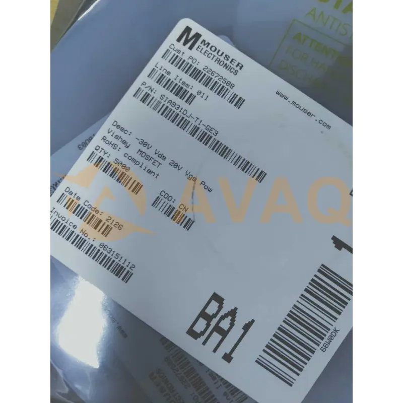
SIA931DJ-T1-GE3
Datasheet:
Part Life Cycle Code:
Active
ECCN Code:
EAR99
Factory Lead Time:
68 Weeks
Case Connection:
DRAIN
EDA/CAD Models:
Send all BOMs to ![]() [email protected],
or fill out the form below for a quote on SIA931DJ-T1-GE3. Guaranteed response within
[email protected],
or fill out the form below for a quote on SIA931DJ-T1-GE3. Guaranteed response within
![]() 12hr.
12hr.
Please fill in the short form below and we will provide you the quotation immediately.
Mosfet Array 30V 4.5A 7.8W Surface Mount PowerPAK® SC-70-6 Dual
| Part Life Cycle Code | Active | Reach Compliance Code | |
| ECCN Code | EAR99 | Factory Lead Time | 68 Weeks |
| Case Connection | DRAIN | Configuration | SEPARATE, 2 ELEMENTS WITH BUILT-IN DIODE |
| DS Breakdown Voltage-Min | 30 V | Drain Current-Max (ID) | 4.5 A |
| Drain-source On Resistance-Max | 0.065 Ω | FET Technology | METAL-OXIDE SEMICONDUCTOR |
| Feedback Cap-Max (Crss) | 45 pF | JESD-30 Code | S-PDSO-N6 |
| Number of Elements | 2 | Number of Terminals | 6 |
| Operating Mode | ENHANCEMENT MODE | Operating Temperature-Max | 150 °C |
| Operating Temperature-Min | -55 °C | Peak Reflow Temperature (Cel) | NOT SPECIFIED |
| Polarity/Channel Type | P-CHANNEL | Power Dissipation-Max (Abs) | 7.8 W |
| Surface Mount | YES | Terminal Form | NO LEAD |
| Terminal Position | DUAL | Time@Peak Reflow Temperature-Max (s) | NOT SPECIFIED |
| Transistor Application | SWITCHING | Transistor Element Material | SILICON |
After-Sales & Settlement Related
 Payment
Payment Method


For alternative payment channels, please reach out to us at:
[email protected] Shipping & Packing
Shipping Method


AVAQ determines and packages all devices based on electrostatic discharge (ESD) and moisture sensitivity level (MSL) protection requirements.
 Warranty

365-Day Product
Quality Guarantee
We promise to provide 365 days quality assurance service for all our products.
| Qty. | Unit Price | Ext. Price |
|---|---|---|
| 1+ | - | - |
The prices below are for reference only.
