Payment Method


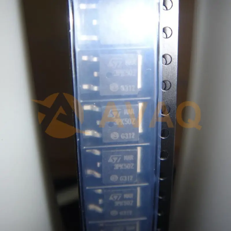
High-Voltage Power MOSFET with P-Channel Configuration
DPAKManufacturer:
Mfr.Part #:
STD3PK50Z
Datasheet:
Part Life Cycle Code:
Obsolete
Pin Count:
3
Reach Compliance Code:
compliant
ECCN Code:
EAR99
EDA/CAD Models:
All bill of materials (BOM) can be sent via email to ![]() [email protected],
or fill below form to Quote for STD3PK50Z, guaranteed quotes back within
[email protected],
or fill below form to Quote for STD3PK50Z, guaranteed quotes back within
![]() 12hr.
12hr.
Please fill in the short form below and we will provide you the quotation immediately.
P-Channel 500 V 2.8A (Tc) 70W (Tc) Surface Mount DPAK
| Source Content uid | STD3PK50Z | Part Life Cycle Code | Obsolete |
| Pin Count | 3 | Reach Compliance Code | compliant |
| ECCN Code | EAR99 | Configuration | SINGLE WITH BUILT-IN DIODE |
| DS Breakdown Voltage-Min | 500 V | Drain Current-Max (ID) | 2.8 A |
| Drain-source On Resistance-Max | 4 Ω | FET Technology | METAL-OXIDE SEMICONDUCTOR |
| JEDEC-95 Code | TO-252 | JESD-30 Code | R-PSSO-G2 |
| JESD-609 Code | e3 | Moisture Sensitivity Level | 1 |
| Number of Elements | 1 | Number of Terminals | 2 |
| Operating Mode | ENHANCEMENT MODE | Operating Temperature-Max | 150 °C |
| Operating Temperature-Min | -55 °C | Peak Reflow Temperature (Cel) | 260 |
| Polarity/Channel Type | P-CHANNEL | Power Dissipation-Max (Abs) | 70 W |
| Pulsed Drain Current-Max (IDM) | 11.2 A | Surface Mount | YES |
| Terminal Finish | MATTE TIN | Terminal Form | GULL WING |
| Terminal Position | SINGLE | Time@Peak Reflow Temperature-Max (s) | 30 |
| Transistor Application | SWITCHING | Transistor Element Material | SILICON |
After-Sales & Settlement Related
 Payment
Payment Method


For alternative payment channels, please reach out to us at:
[email protected] Shipping & Packing
Shipping Method


AVAQ determines and packages all devices based on electrostatic discharge (ESD) and moisture sensitivity level (MSL) protection requirements.
 Warranty

365-Day Product
Quality Guarantee
We promise to provide 365 days quality assurance service for all our products.
| Qty. | Unit Price | Ext. Price |
|---|---|---|
| 1+ | - | - |
The prices below are for reference only.
