Payment Method


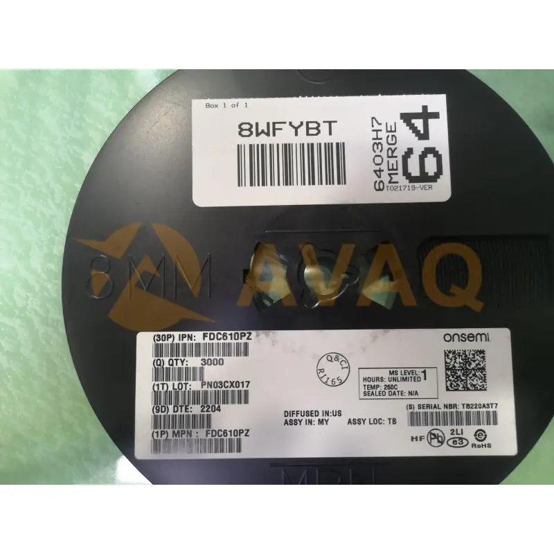
The FDC610PZ is a P-channel MOSFET designed for a maximum voltage of 30V and a current of 4.9A, contained within a 6-pin TSOT-23 package
TSOT-23-6Manufacturer:
Mfr.Part #:
FDC610PZ
Datasheet:
Pbfree Code:
Yes
Part Life Cycle Code:
Active
Reach Compliance Code:
compliant
ECCN Code:
EAR99
EDA/CAD Models:
Send all BOMs to ![]() [email protected],
or fill out the form below for a quote on FDC610PZ. Guaranteed response within
[email protected],
or fill out the form below for a quote on FDC610PZ. Guaranteed response within
![]() 12hr.
12hr.
Please fill in the short form below and we will provide you the quotation immediately.
The FDC610PZ is a high-performance Channel MOSFET designed for battery power applications. Utilizing advanced PowerTrench® technology, this MOSFET boasts minimal on state resistance and low gate charge, ensuring superior switching performance. Its versatility makes it well-suited for a range of applications, including load switching, power management, battery charging circuits, and DC/DC conversion. With its optimized design, the FDC610PZ is an ideal choice for engineers and designers looking for reliable and efficient solutions for their power needs
| Source Content uid | FDC610PZ | Pbfree Code | Yes |
| Part Life Cycle Code | Active | Reach Compliance Code | compliant |
| ECCN Code | EAR99 | HTS Code | 8541.29.00.95 |
| Factory Lead Time | 46 Weeks | Configuration | SINGLE WITH BUILT-IN DIODE |
| DS Breakdown Voltage-Min | 30 V | Drain Current-Max (ID) | 0.0049 A |
| Drain-source On Resistance-Max | 0.042 Ω | FET Technology | METAL-OXIDE SEMICONDUCTOR |
| Feedback Cap-Max (Crss) | 190 pF | JESD-30 Code | R-PDSO-G6 |
| JESD-609 Code | e3 | Moisture Sensitivity Level | 1 |
| Number of Elements | 1 | Number of Terminals | 6 |
| Operating Mode | ENHANCEMENT MODE | Operating Temperature-Max | 150 °C |
| Operating Temperature-Min | -55 °C | Peak Reflow Temperature (Cel) | 260 |
| Polarity/Channel Type | P-CHANNEL | Power Dissipation Ambient-Max | 1.6 W |
| Power Dissipation-Max (Abs) | 1.6 W | Qualification Status | Not Qualified |
| Surface Mount | YES | Terminal Finish | MATTE TIN |
| Terminal Form | GULL WING | Terminal Position | DUAL |
| Time@Peak Reflow Temperature-Max (s) | 30 | Transistor Application | SWITCHING |
| Transistor Element Material | SILICON |
After-Sales & Settlement Related
 Payment
Payment Method


For alternative payment channels, please reach out to us at:
[email protected] Shipping & Packing
Shipping Method


AVAQ determines and packages all devices based on electrostatic discharge (ESD) and moisture sensitivity level (MSL) protection requirements.
 Warranty

365-Day Product
Quality Guarantee
We promise to provide 365 days quality assurance service for all our products.
| Qty. | Unit Price | Ext. Price |
|---|---|---|
| 1+ | - | - |
The prices below are for reference only.
