Payment Method


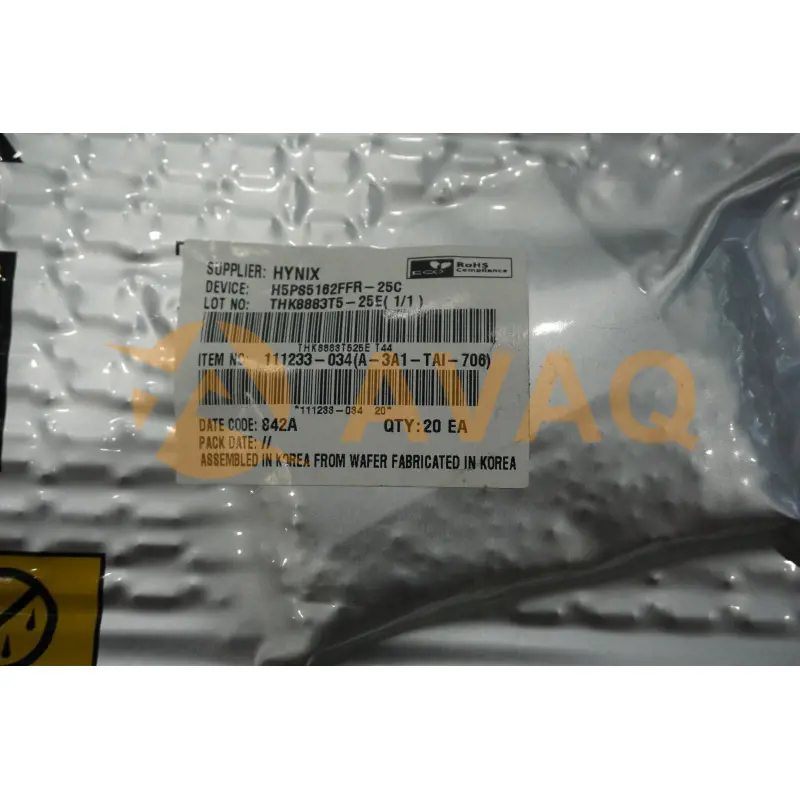
DDR DRAM with a capacity of 32MX16 and a latency of 0.5ns
BGA84Manufacturer:
SK HYNIX INC
Mfr.Part #:
H5PS5162FFR-25C
Datasheet:
Part Life Cycle Code:
Obsolete
Pin Count:
84
ECCN Code:
EAR99
HTS Code:
8542.32.00.28
EDA/CAD Models:
Send all BOMs to ![]() [email protected],
or fill out the form below for a quote on H5PS5162FFR-25C. Guaranteed response within
[email protected],
or fill out the form below for a quote on H5PS5162FFR-25C. Guaranteed response within
![]() 12hr.
12hr.
Please fill in the short form below and we will provide you the quotation immediately.
| Part Life Cycle Code | Obsolete | Pin Count | 84 |
| Reach Compliance Code | ECCN Code | EAR99 | |
| HTS Code | 8542.32.00.28 | Access Mode | FOUR BANK PAGE BURST |
| Access Time-Max | 0.5 ns | Additional Feature | AUTO/SELF REFRESH |
| Clock Frequency-Max (fCLK) | 400 MHz | I/O Type | COMMON |
| Interleaved Burst Length | 4,8 | JESD-30 Code | R-PBGA-B208 |
| JESD-609 Code | e1 | Length | 13 mm |
| Memory Density | 536870912 bit | Memory IC Type | DDR2 DRAM |
| Memory Width | 16 | Number of Functions | 1 |
| Number of Ports | 1 | Number of Terminals | 84 |
| Number of Words | 33554432 words | Number of Words Code | 32000000 |
| Operating Mode | SYNCHRONOUS | Operating Temperature-Max | 85 °C |
| Operating Temperature-Min | Organization | 32MX16 | |
| Output Characteristics | 3-STATE | Peak Reflow Temperature (Cel) | 260 |
| Qualification Status | Not Qualified | Refresh Cycles | 8192 |
| Seated Height-Max | 1.2 mm | Self Refresh | YES |
| Sequential Burst Length | 4,8 | Standby Current-Max | 0.008 A |
| Supply Current-Max | 0.28 mA | Supply Voltage-Max (Vsup) | 1.9 V |
| Supply Voltage-Min (Vsup) | 1.7 V | Supply Voltage-Nom (Vsup) | 1.8 V |
| Surface Mount | YES | Technology | CMOS |
| Temperature Grade | OTHER | Terminal Finish | Tin/Silver/Copper (Sn96.5Ag3.0Cu0.5) |
| Terminal Form | BALL | Terminal Pitch | 0.8 mm |
| Terminal Position | BOTTOM | Time@Peak Reflow Temperature-Max (s) | 20 |
| Width | 8 mm |
After-Sales & Settlement Related
 Payment
Payment Method


For alternative payment channels, please reach out to us at:
[email protected] Shipping & Packing
Shipping Method


AVAQ determines and packages all devices based on electrostatic discharge (ESD) and moisture sensitivity level (MSL) protection requirements.
 Warranty

365-Day Product
Quality Guarantee
We promise to provide 365 days quality assurance service for all our products.
| Qty. | Unit Price | Ext. Price |
|---|---|---|
| 1+ | - | - |
The prices below are for reference only.

AK1573
Asahi Kasei Microdevices/AKM
1000+ $2.489

MN3102
Panasonic
Durable Plastic Package for Moisture-Sensitive Environments

SI5351A-B-GT
Skyworks
Clock Generator Si5351A-B-GT PK

LMX2594RHAT
Texas Instruments
15-GHz wideband PLLatinum™ RF synthesizer with phase synchronization and JESD204B support 40-VQFN -40 to 85"

LM565CN
Texas Instruments
PLL Single 0.25MHz to 0.5MHz 14-Pin MDIP Rail
