Payment Method


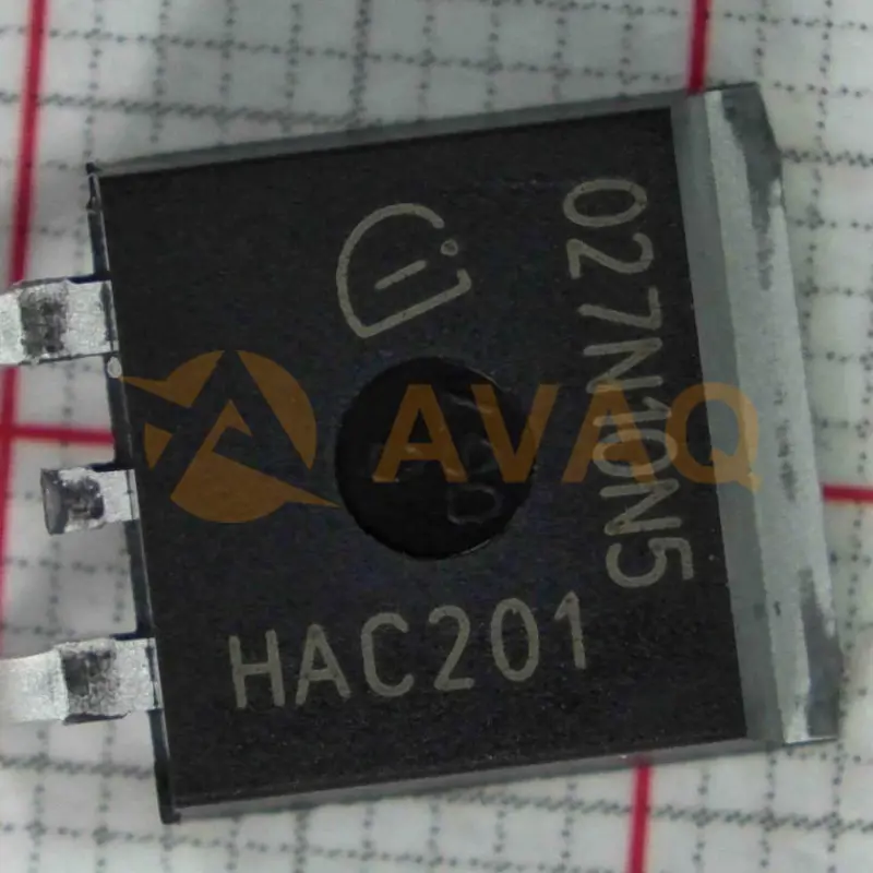
High-power switching device for efficient voltage regulation
D2PAK (TO-263)Manufacturer:
Mfr.Part #:
IPB027N10N5
Datasheet:
Part Life Cycle Code:
Active
Reach Compliance Code:
compliant
ECCN Code:
EAR99
Avalanche Energy Rating (Eas):
461 mJ
EDA/CAD Models:
Send all BOMs to ![]() [email protected],
or fill out the form below for a quote on IPB027N10N5. Guaranteed response within
[email protected],
or fill out the form below for a quote on IPB027N10N5. Guaranteed response within
![]() 12hr.
12hr.
Please fill in the short form below and we will provide you the quotation immediately.
The IPB027N10N5 OptiMOS™ 5 100V power MOSFET by Infineon is designed to meet the demanding requirements of synchronous rectification in telecom blocks and server power supply applications. Its lower RDS(on) of 22% compared to similar devices sets it apart, making it a top choice for applications where power density and efficiency are crucial. These features, combined with its low on-state resistance, make it an industry-leading solution for Or-ing, hotswap, and battery protection needs in the telecom and server power sectors
| Source Content uid | IPB027N10N5 | Part Life Cycle Code | Active |
| Reach Compliance Code | compliant | ECCN Code | EAR99 |
| Avalanche Energy Rating (Eas) | 461 mJ | Case Connection | DRAIN |
| Configuration | SINGLE WITH BUILT-IN DIODE | DS Breakdown Voltage-Min | 100 V |
| Drain Current-Max (ID) | 120 A | Drain-source On Resistance-Max | 0.0027 Ω |
| FET Technology | METAL-OXIDE SEMICONDUCTOR | JEDEC-95 Code | TO-263AB |
| JESD-30 Code | R-PSSO-G2 | JESD-609 Code | e3 |
| Moisture Sensitivity Level | 1 | Number of Elements | 1 |
| Number of Terminals | 2 | Operating Mode | ENHANCEMENT MODE |
| Polarity/Channel Type | N-CHANNEL | Pulsed Drain Current-Max (IDM) | 480 A |
| Surface Mount | YES | Terminal Finish | TIN |
| Terminal Form | GULL WING | Terminal Position | SINGLE |
| Transistor Application | SWITCHING | Transistor Element Material | SILICON |
| Product Category | MOSFET | Technology | Si |
| Mounting Style | SMD/SMT | Height | 4.4 mm |
| Length | 10 mm | Product Type | MOSFET |
| Subcategory | MOSFETs | Width | 9.25 mm |
| Unit Weight | 0.139332 oz |
After-Sales & Settlement Related
 Payment
Payment Method


For alternative payment channels, please reach out to us at:
[email protected] Shipping & Packing
Shipping Method


AVAQ determines and packages all devices based on electrostatic discharge (ESD) and moisture sensitivity level (MSL) protection requirements.
 Warranty

365-Day Product
Quality Guarantee
We promise to provide 365 days quality assurance service for all our products.
| Qty. | Unit Price | Ext. Price |
|---|---|---|
| 1+ | $4.328 | $4.33 |
| 10+ | $3.779 | $37.79 |
| 30+ | $3.454 | $103.62 |
| 100+ | $3.124 | $312.40 |
| 500+ | $2.972 | $1,486.00 |
| 1000+ | $2.903 | $2,903.00 |
The prices below are for reference only.
