Payment Method


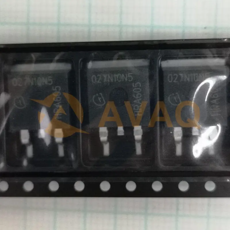
Power MOSFET, 120A current rating, 100V voltage, low 0.0027 ohm resistance, N-channel
TO-263-3Manufacturer:
Mfr.Part #:
IPB027N10N5ATMA1
Datasheet:
Pbfree Code:
Yes
Part Life Cycle Code:
Active
Reach Compliance Code:
not_compliant
ECCN Code:
EAR99
EDA/CAD Models:
Send all BOMs to ![]() [email protected],
or fill out the form below for a quote on IPB027N10N5ATMA1. Guaranteed response within
[email protected],
or fill out the form below for a quote on IPB027N10N5ATMA1. Guaranteed response within
![]() 12hr.
12hr.
Please fill in the short form below and we will provide you the quotation immediately.
The IPB027N10N5ATMA1 stands out with a myriad of features tailored for modern power management needs. Optimized specifically for synchronous rectification, these MOSFETs shine in environments demanding high switching frequencies. Notably, they offer a remarkable reduction in output capacitance by up to 44%, alongside a substantial 43% decrease in RDS(on) compared to the previous generation. These enhancements translate into tangible benefits for system efficiency, switching and conduction losses reduction, minimized need for paralleling, heightened power density, and mitigated voltage overshoot
| Pbfree Code | Yes | Part Life Cycle Code | Active |
| Reach Compliance Code | not_compliant | ECCN Code | EAR99 |
| Factory Lead Time | 52 Weeks | Avalanche Energy Rating (Eas) | 461 mJ |
| Case Connection | DRAIN | Configuration | SINGLE WITH BUILT-IN DIODE |
| DS Breakdown Voltage-Min | 100 V | Drain Current-Max (ID) | 120 A |
| Drain-source On Resistance-Max | 0.0027 Ω | FET Technology | METAL-OXIDE SEMICONDUCTOR |
| JEDEC-95 Code | TO-263AB | JESD-30 Code | R-PSSO-G2 |
| JESD-609 Code | e3 | Moisture Sensitivity Level | 1 |
| Number of Elements | 1 | Number of Terminals | 2 |
| Operating Mode | ENHANCEMENT MODE | Polarity/Channel Type | N-CHANNEL |
| Pulsed Drain Current-Max (IDM) | 480 A | Surface Mount | YES |
| Terminal Finish | TIN | Terminal Form | GULL WING |
| Terminal Position | SINGLE | Transistor Application | SWITCHING |
| Transistor Element Material | SILICON | Series | OptiMOS™ |
| FET Type | N-Channel | Technology | MOSFET (Metal Oxide) |
| Drain to Source Voltage (Vdss) | 100 V | Current - Continuous Drain (Id) @ 25°C | 120A (Tc) |
| Drive Voltage (Max Rds On, Min Rds On) | 6V, 10V | Rds On (Max) @ Id, Vgs | 2.7mOhm @ 100A, 10V |
| Vgs(th) (Max) @ Id | 3.8V @ 184µA | Gate Charge (Qg) (Max) @ Vgs | 139 nC @ 10 V |
| Vgs (Max) | ±20V | Input Capacitance (Ciss) (Max) @ Vds | 10300 pF @ 50 V |
| Power Dissipation (Max) | 250W (Tc) | Operating Temperature | -55°C ~ 175°C (TJ) |
| Mounting Type | Surface Mount | Base Product Number | IPB027 |
After-Sales & Settlement Related
 Payment
Payment Method


For alternative payment channels, please reach out to us at:
[email protected] Shipping & Packing
Shipping Method


AVAQ determines and packages all devices based on electrostatic discharge (ESD) and moisture sensitivity level (MSL) protection requirements.
 Warranty

365-Day Product
Quality Guarantee
We promise to provide 365 days quality assurance service for all our products.
| Qty. | Unit Price | Ext. Price |
|---|---|---|
| 1+ | - | - |
The prices below are for reference only.
