Payment Method


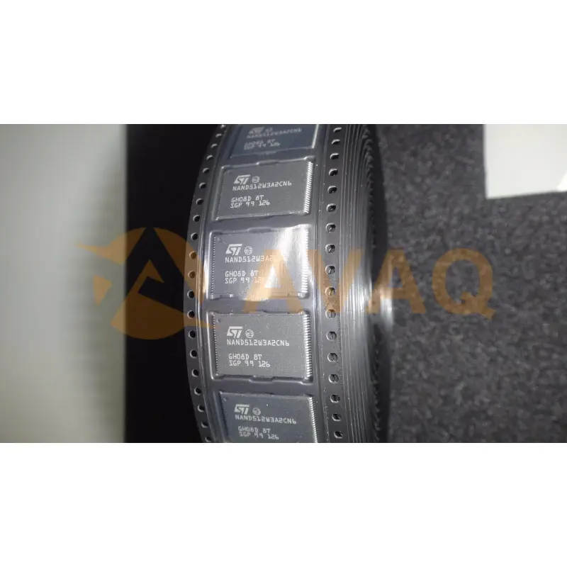
8 NAND512W3A2CN6F with 64Mx8 flash configuration and 35ns speed
TSOPManufacturer:
Micron Technology
Mfr.Part #:
NAND512W3A2CN6F
Datasheet:
Part Life Cycle Code:
Transferred
Pin Count:
48
Reach Compliance Code:
compliant
ECCN Code:
EAR99
EDA/CAD Models:
All bill of materials (BOM) can be sent via email to ![]() [email protected],
or fill below form to Quote for NAND512W3A2CN6F, guaranteed quotes back within
[email protected],
or fill below form to Quote for NAND512W3A2CN6F, guaranteed quotes back within
![]() 12hr.
12hr.
Please fill in the short form below and we will provide you the quotation immediately.
SUMMARY DESCRIPTIONThe NAND Flash 528 Byte/ 264 Word Page is a family of non-volatile Flash memories that usesthe Single Level Cell (SLC) NAND cell technology. It is referred to as the Small Page family. The devices range from 128Mbits to 1Gbit and operate with either a 1.8V or 3V voltage supply. The size of a Page is either 528 Bytes (512 + 16 spare) or 264 Words (256 + 8 spare) depending on whether the device has a x8 or x16 bus width.FEATURES SUMMARY■ HIGH DENSITY NAND FLASH MEMORIES – Up to 1 Gbit memory array – Up to 32 Mbit spare area – Cost effective solutions for mass storage applications■ NAND INTERFACE – x8 or x16 bus width – Multiplexed Address/ Data – Pinout compatibility for all densities■ SUPPLY VOLTAGE – 1.8V device: VDD = 1.7 to 1.95V – 3.0V device: VDD = 2.7 to 3.6V■ PAGE SIZE – x8 device: (512 + 16 spare) Bytes – x16 device: (256 + 8 spare) Words■ BLOCK SIZE – x8 device: (16K + 512 spare) Bytes – x16 device: (8K + 256 spare) Words■ PAGE READ / PROGRAM – Random access: 12µs (max) – Sequential access: 50ns (min) – Page program time: 200µs (typ)■ COPY BACK PROGRAM MODE – Fast page copy without external buffering■ FAST BLOCK ERASE – Block erase time: 2ms (Typ)■ STATUS REGISTER■ ELECTRONIC SIGNATURE■ CHIP ENABLE ‘DON’T CARE’ OPTION – Simple interface with microcontroller■ SERIAL NUMBER OPTION■ HARDWARE DATA PROTECTION – Program/Erase locked during Power transitions■ DATA INTEGRITY – 100,000 Program/Erase cycles – 10 years Data Retention■ RoHS COMPLIANCE – Lead-Free Components are Compliant with the RoHS Directive■ DEVELOPMENT TOOLS – Error Correction Code software and hardware models – Bad Blocks Management and Wear Leveling algorithms – File System OS Native reference software – Hardware simulation models
| Source Content uid | NAND512W3A2CN6F | Part Life Cycle Code | Transferred |
| Pin Count | 48 | Reach Compliance Code | compliant |
| ECCN Code | EAR99 | HTS Code | 8542.32.00.51 |
| Access Time-Max | 12000 ns | Command User Interface | YES |
| Data Polling | NO | JESD-30 Code | R-PDSO-G48 |
| JESD-609 Code | e3/e6 | Length | 18.4 mm |
| Memory Density | 536870912 bit | Memory IC Type | FLASH |
| Memory Width | 8 | Number of Functions | 1 |
| Number of Sectors/Size | 4K | Number of Terminals | 48 |
| Number of Words | 67108864 words | Number of Words Code | 64000000 |
| Operating Mode | ASYNCHRONOUS | Operating Temperature-Max | 85 °C |
| Operating Temperature-Min | -40 °C | Organization | 64MX8 |
| Page Size | 512 words | Parallel/Serial | PARALLEL |
| Peak Reflow Temperature (Cel) | 260 | Programming Voltage | 3 V |
| Qualification Status | Not Qualified | Ready/Busy | YES |
| Seated Height-Max | 1.2 mm | Sector Size | 16K |
| Standby Current-Max | 0.00005 A | Supply Current-Max | 0.02 mA |
| Supply Voltage-Max (Vsup) | 3.6 V | Supply Voltage-Min (Vsup) | 2.7 V |
| Supply Voltage-Nom (Vsup) | 3 V | Surface Mount | YES |
| Technology | CMOS | Temperature Grade | INDUSTRIAL |
| Terminal Finish | TIN/TIN BISMUTH | Terminal Form | GULL WING |
| Terminal Pitch | 0.5 mm | Terminal Position | DUAL |
| Time@Peak Reflow Temperature-Max (s) | NOT SPECIFIED | Toggle Bit | NO |
| Type | SLC NAND TYPE | Width | 12 mm |
After-Sales & Settlement Related
 Payment
Payment Method


For alternative payment channels, please reach out to us at:
[email protected] Shipping & Packing
Shipping Method


AVAQ determines and packages all devices based on electrostatic discharge (ESD) and moisture sensitivity level (MSL) protection requirements.
 Warranty

365-Day Product
Quality Guarantee
We promise to provide 365 days quality assurance service for all our products.
| Qty. | Unit Price | Ext. Price |
|---|---|---|
| 1+ | - | - |
The prices below are for reference only.
