Payment Method


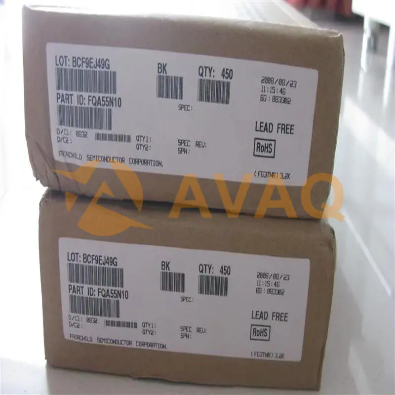
MOSFET 100V N-Channel QFET
TO-3PManufacturer:
onsemi
Mfr.Part #:
FQA55N10
Datasheet:
Technology:
Si
Mounting Style:
Through Hole
Transistor Polarity:
N-Channel
Number Of Channels:
1 Channel
EDA/CAD Models:
Send all BOMs to ![]() [email protected],
or fill out the form below for a quote on FQA55N10. Guaranteed response within
[email protected],
or fill out the form below for a quote on FQA55N10. Guaranteed response within
![]() 12hr.
12hr.
Please fill in the short form below and we will provide you the quotation immediately.
N-Channel 100 V 61A (Tc) 190W (Tc) Through Hole TO-3P
| Product Category | MOSFET | Technology | Si |
| Mounting Style | Through Hole | Transistor Polarity | N-Channel |
| Number of Channels | 1 Channel | Vds - Drain-Source Breakdown Voltage | 100 V |
| Id - Continuous Drain Current | 61 A | Rds On - Drain-Source Resistance | 26 mOhms |
| Vgs - Gate-Source Voltage | - 25 V, + 25 V | Minimum Operating Temperature | - 55 C |
| Maximum Operating Temperature | + 175 C | Pd - Power Dissipation | 190 W |
| Channel Mode | Enhancement | Configuration | Single |
| Fall Time | 140 ns | Forward Transconductance - Min | 39 S |
| Height | 20.1 mm | Length | 16.2 mm |
| Product Type | MOSFET | Rise Time | 250 ns |
| Factory Pack Quantity | 450 | Subcategory | MOSFETs |
| Transistor Type | 1 N-Channel | Type | MOSFET |
| Typical Turn-Off Delay Time | 110 ns | Typical Turn-On Delay Time | 25 ns |
| Width | 5 mm | Part # Aliases | FQA55N10_NL |
| Unit Weight | 0.162260 oz |
After-Sales & Settlement Related
 Payment
Payment Method


For alternative payment channels, please reach out to us at:
[email protected] Shipping & Packing
Shipping Method


AVAQ determines and packages all devices based on electrostatic discharge (ESD) and moisture sensitivity level (MSL) protection requirements.
 Warranty

365-Day Product
Quality Guarantee
We promise to provide 365 days quality assurance service for all our products.
| Qty. | Unit Price | Ext. Price |
|---|---|---|
| 1+ | - | - |
The prices below are for reference only.
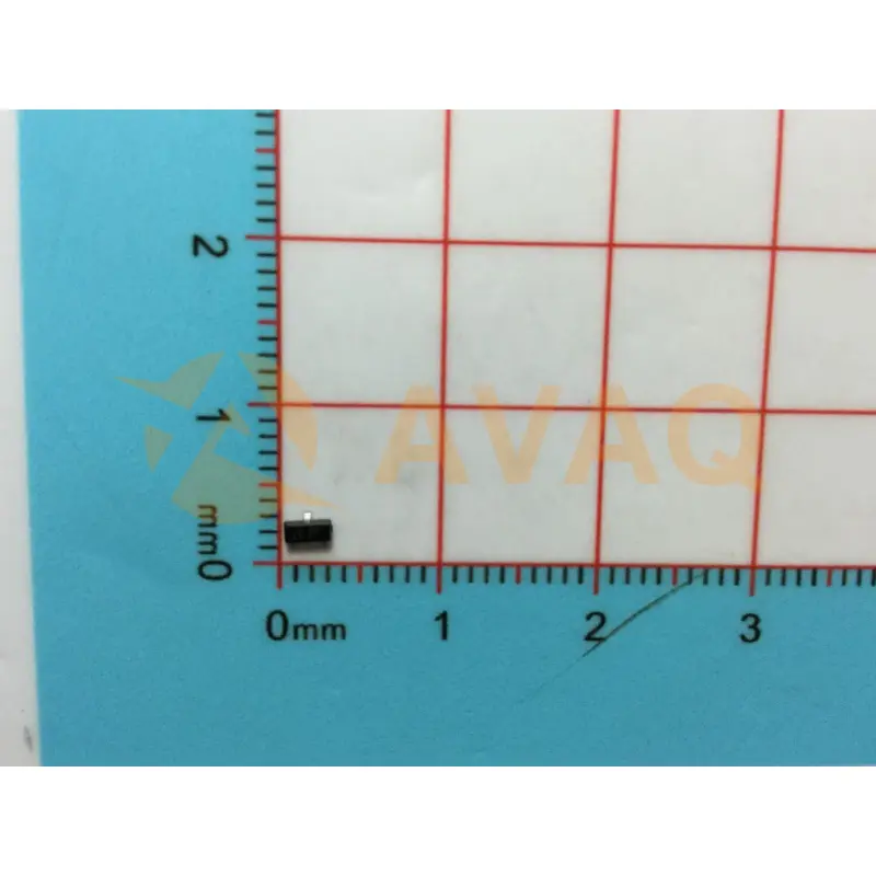
2N2222
Stmicroelectronics
1000+ $0.587
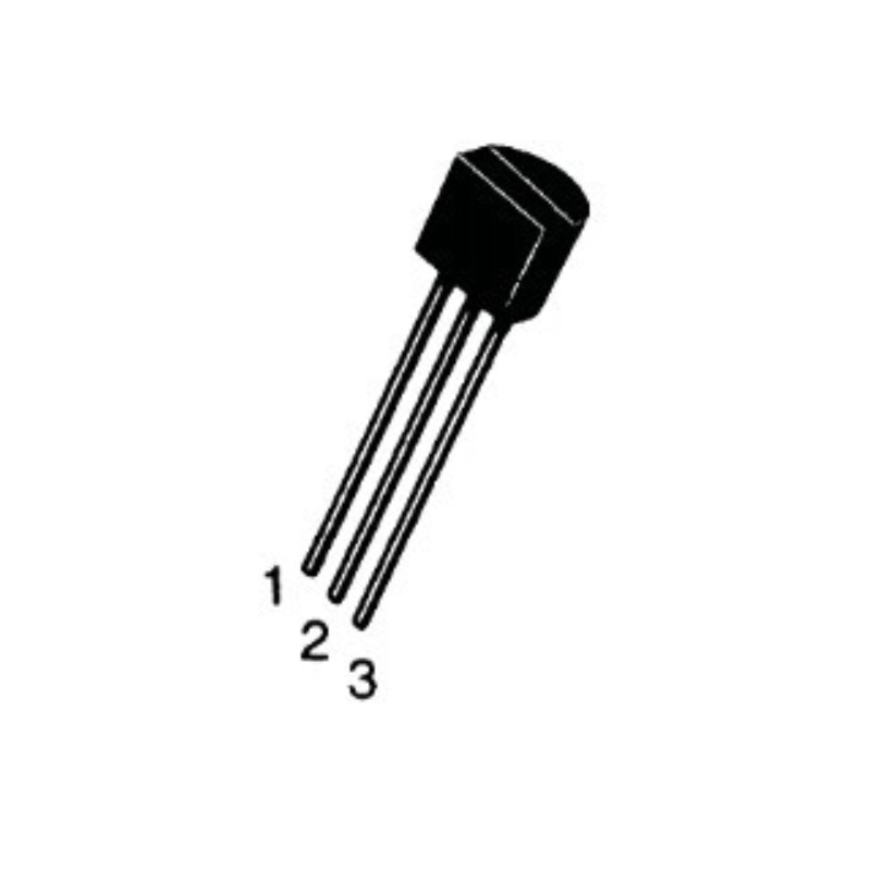
BC547
Onsemi
NPN Epitaxial Silicon Transistor
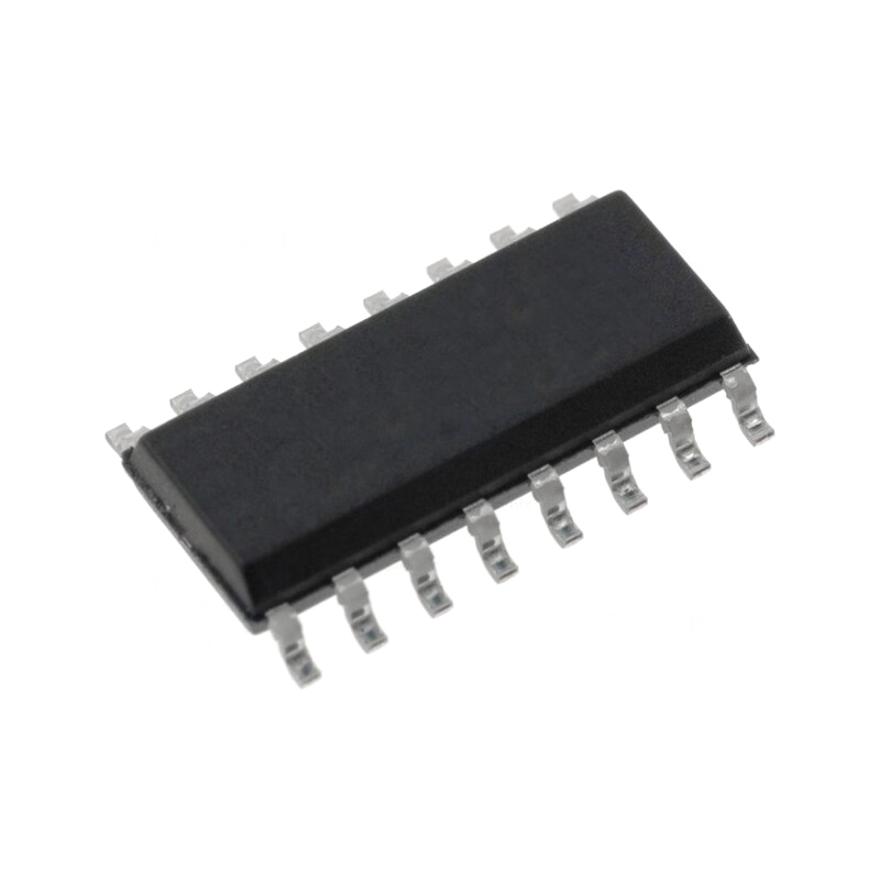
ULN2003
Onsemi
Versatile device for driving heavy loads and motor
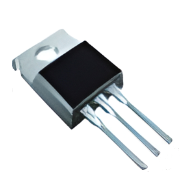
IRF3205
Infineon
TO-220AB Tube Power Transistor with N-Channel Silicon

TAN15
Microchip
The TAN is a robust NPN transistor designed for high-frequency applications, capable of operating at up to V and continuous curren
