Payment Method


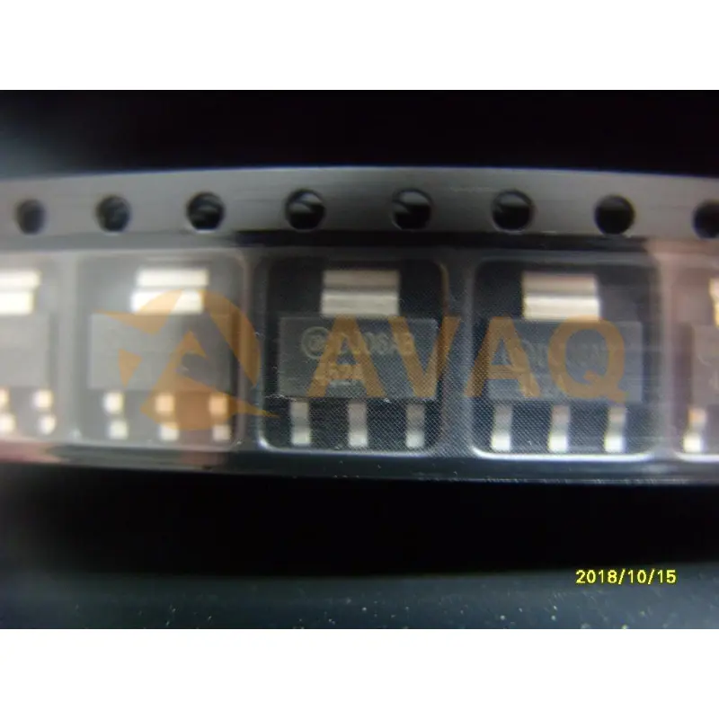
P-Channel Enhancement Mode Field Effect Transistor -30V, -5A, 65mΩ
SOT-223Manufacturer:
Fairchild Semiconductor
Mfr.Part #:
NDT452AP
Datasheet:
Pbfree Code:
Yes
Part Life Cycle Code:
Active
Reach Compliance Code:
not_compliant
ECCN Code:
EAR99
EDA/CAD Models:
Send all BOMs to ![]() [email protected],
or fill out the form below for a quote on NDT452AP. Guaranteed response within
[email protected],
or fill out the form below for a quote on NDT452AP. Guaranteed response within
![]() 12hr.
12hr.
Please fill in the short form below and we will provide you the quotation immediately.
The ON Semiconductor NDT452AP is a Power SOT P-Channel enhancement mode power field effect transistor that utilizes the latest DMOS technology to deliver superior performance in low voltage applications. With its high cell density design, this transistor minimizes on-state resistance and ensures excellent switching capabilities, making it ideal for use in notebook computer power management and DC motor control. Whether you're designing a system that requires efficient power management or looking to enhance the performance of your DC motor control applications, the NDT452AP offers the reliability and precision you need
| Source Content uid | NDT452AP | Pbfree Code | Yes |
| Part Life Cycle Code | Active | Reach Compliance Code | not_compliant |
| ECCN Code | EAR99 | Factory Lead Time | 55 Weeks |
| Case Connection | DRAIN | Configuration | SINGLE WITH BUILT-IN DIODE |
| DS Breakdown Voltage-Min | 30 V | Drain Current-Max (ID) | 5 A |
| Drain-source On Resistance-Max | 0.065 Ω | FET Technology | METAL-OXIDE SEMICONDUCTOR |
| JESD-30 Code | R-PDSO-G4 | JESD-609 Code | e3 |
| Moisture Sensitivity Level | 1 | Number of Elements | 1 |
| Number of Terminals | 4 | Operating Mode | ENHANCEMENT MODE |
| Operating Temperature-Max | 150 °C | Operating Temperature-Min | -65 °C |
| Peak Reflow Temperature (Cel) | 260 | Polarity/Channel Type | P-CHANNEL |
| Power Dissipation-Max (Abs) | 3 W | Pulsed Drain Current-Max (IDM) | 15 A |
| Qualification Status | Not Qualified | Surface Mount | YES |
| Terminal Finish | MATTE TIN | Terminal Form | GULL WING |
| Terminal Position | DUAL | Time@Peak Reflow Temperature-Max (s) | 30 |
| Transistor Application | SWITCHING | Transistor Element Material | SILICON |
After-Sales & Settlement Related
 Payment
Payment Method


For alternative payment channels, please reach out to us at:
[email protected] Shipping & Packing
Shipping Method


AVAQ determines and packages all devices based on electrostatic discharge (ESD) and moisture sensitivity level (MSL) protection requirements.
 Warranty

365-Day Product
Quality Guarantee
We promise to provide 365 days quality assurance service for all our products.
| Qty. | Unit Price | Ext. Price |
|---|---|---|
| 1+ | - | - |
The prices below are for reference only.
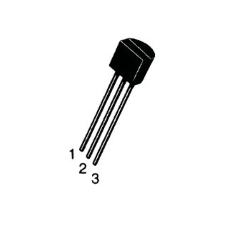
2N2222
Stmicroelectronics
1000+ $0.587
BC547
Onsemi
NPN Epitaxial Silicon Transistor
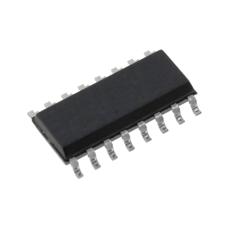
ULN2003
Onsemi
Versatile device for driving heavy loads and motor
IRF3205
Infineon
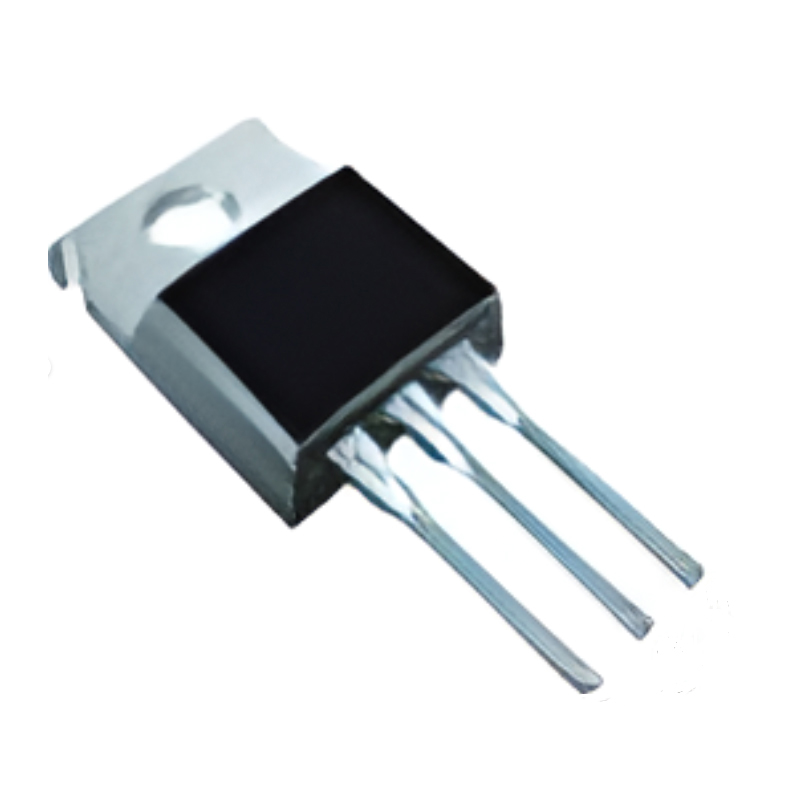
TO-220AB Tube Power Transistor with N-Channel Silicon

TAN15
Microchip
The TAN is a robust NPN transistor designed for high-frequency applications, capable of operating at up to V and continuous curren
